- 您現(xiàn)在的位置:買賣IC網(wǎng) > PDF目錄51253 > AGR19090EF (TRIQUINT SEMICONDUCTOR INC) L BAND, Si, N-CHANNEL, RF POWER, MOSFET PDF資料下載
參數(shù)資料
| 型號: | AGR19090EF |
| 廠商: | TRIQUINT SEMICONDUCTOR INC |
| 元件分類: | 功率晶體管 |
| 英文描述: | L BAND, Si, N-CHANNEL, RF POWER, MOSFET |
| 文件頁數(shù): | 1/10頁 |
| 文件大小: | 366K |
| 代理商: | AGR19090EF |
AGR19090E
90 W, 1930 MHz—1990 MHz, PCS LDMOS RF Power Transistor
Introduction
The AGR19090E is a 90 W, 28 V N-channel laterally
diffused metal oxide semiconductor (LDMOS) RF
power field effect transistor (FET) suitable for per-
sonal communication service (PCS) (1930 MHz—
1990 MHz), wide-band code division multiple access
(W-CDMA), global system for mobile communication
(GSM/EDGE), time-division multiple access (TDMA),
and single-carrier or multicarrier class AB power
amplifier applications.
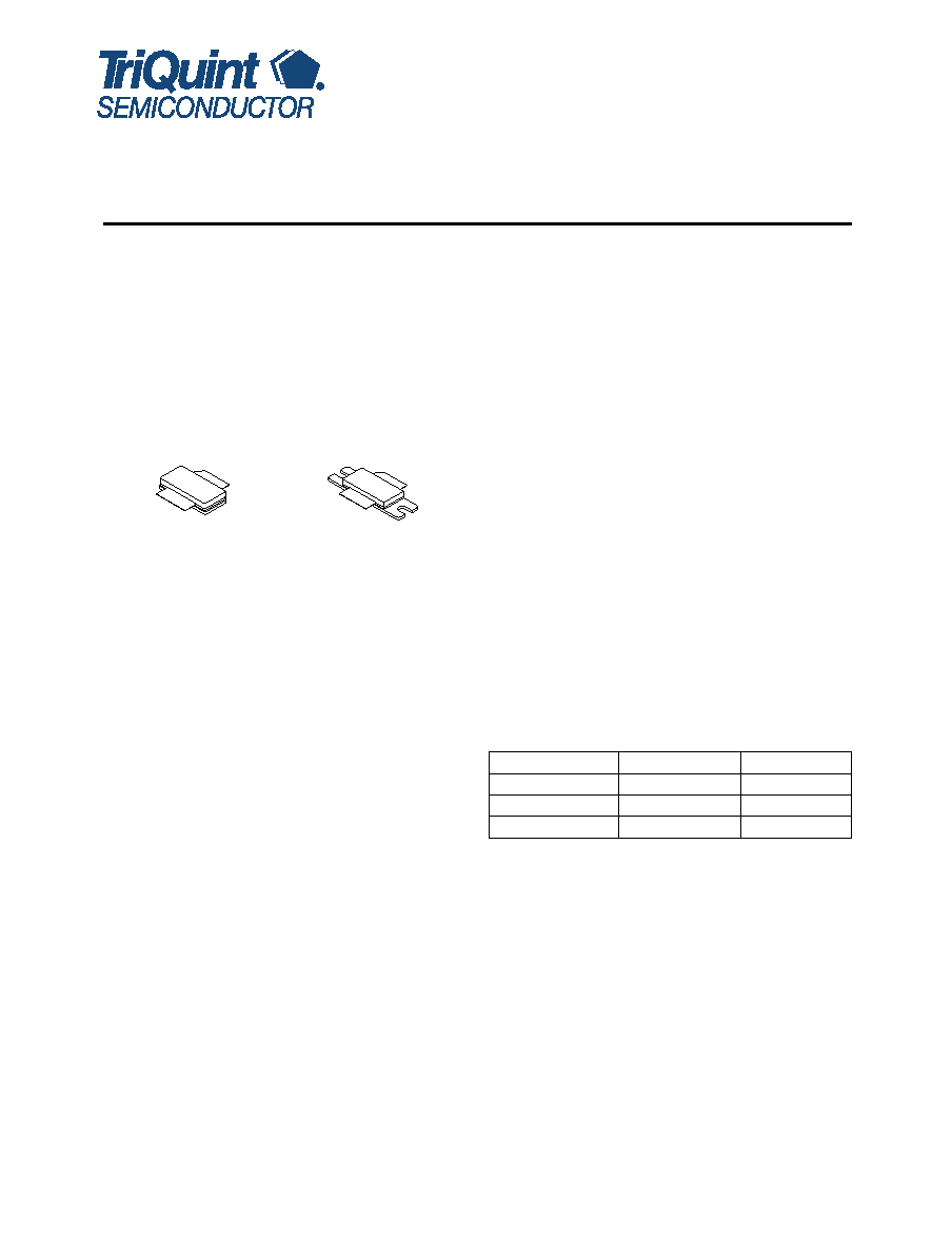
Figure 1. Available Packages
N-CDMA Features
Typical 2 carrier N-CDMA performance: VDD =
28 V, IDQ = 850 mA, f1 = 1958.75 MHz, f2 =
1961.25 MHz, IS-95 CDMA (pilot, sync, paging,
traffic codes 8—13). Peak/average (P/A) = 9.72 dB
at 0.01% probability on CCDF. 1.2288 MHz trans-
mission bandwidth (BW). Adjacent channel power
ratio (ACPR) measured over 30 kHz BW at f1 –
885 kHz and f2 + 885 kHz. Third-order intermodu-
lation (IM3) distortion measured over a
1.2288 MHz BW at f1 – 2.5 MHz and f2 + 2.5 MHz.
— Output power (POUT): 18 W.
— Power gain: 15.0 dB.
— Efficiency: 25.8%.
— IM3: –34.5 dBc.
— ACPR: –50 dBc.
EDGE Features
Typical EDGE performance (1960 MHz, 26 V,
IDQ = 800 mA):
— Output power (POUT): 36 W.
— Power gain: 15.0 dB.
— Efficiency: 38%.
— Modulation spectrum:
@ ±400 kHz = –61.0 dBc.
@ ±600 kHz = –73.0 dBc.
— Error vector magnitude (EVM) = 2.2%.
GSM Features
Typical performance over entire GSM band:
— P1dB: 90 W typical.
— Continuous wave (CW) power gain: @ P1dB =
14.0 dB.
— CW Efficiency @ P1dB = 50% typical.
— Return loss: –12 dB.
Device Performance Features
High-reliability, gold-metalization process.
Low hot carrier injection (HCI) induced bias drift
over 20 years.
Internally matched.
High gain, efficiency, and linearity.
Integrated ESD protection.
Device can withstand 10:1 voltage standing wave
ratio (VSWR) at 28 Vdc, 1930 MHz, 90 W CW
output power.
Large signal impedance parameters available.
ESD Rating*
* Although electrostatic discharge (ESD) protection circuitry has
been designed into this device, proper precautions must be
taken to avoid exposure to ESD and electrical overstress (EOS)
during all handling, assembly, and test operations. Agere
employs a human-body model (HBM), a machine model (MM),
and a charged-device model (CDM) qualification requirement in
order to determine ESD-susceptibility limits and protection
design evaluation. ESD voltage thresholds are dependent on the
circuit parameters used in each of the models, as defined by
JEDEC's JESD22-A114B (HBM), JESD22-A115A (MM), and
JESD22-C101A (CDM) standards.
Caution: MOS devices are susceptible to damage from elec-
trostatic charge. Reasonable precautions in han-
dling and packaging MOS devices should be
observed.
AGR19090EU (unflanged) AGR19090EF (flanged)
AGR19090E
Minimum (V)
Class
HBM
500
1B
MM
50
A
CDM
1500
4
PEAK Devices
相關(guān)PDF資料 |
PDF描述 |
|---|---|
| AGR19125EF | L BAND, Si, N-CHANNEL, RF POWER, MOSFET |
| AGR19125EU | L BAND, Si, N-CHANNEL, RF POWER, MOSFET |
| AGR19180EF | L BAND, Si, N-CHANNEL, RF POWER, MOSFET |
| AGR19180EF | 2 CHANNEL, L BAND, Si, N-CHANNEL, RF POWER, MOSFET |
| AGR19180EF | 2 CHANNEL, L BAND, Si, N-CHANNEL, RF POWER, MOSFET |
相關(guān)代理商/技術(shù)參數(shù) |
參數(shù)描述 |
|---|---|
| AGR19090EU | 制造商:TRIQUINT 制造商全稱:TriQuint Semiconductor 功能描述:90 W, 1930 MHz-1990 MHz, PCS LDMOS RF Power Transistor |
| AGR19125E | 制造商:TRIQUINT 制造商全稱:TriQuint Semiconductor 功能描述:125 W, 1930 MHz-1990 MHz, PCS LDMOS RF Power Transistor |
| AGR19125EF | 功能描述:射頻MOSFET電源晶體管 RF Transistor RoHS:否 制造商:Freescale Semiconductor 配置:Single 晶體管極性: 頻率:1800 MHz to 2000 MHz 增益:27 dB 輸出功率:100 W 汲極/源極擊穿電壓: 漏極連續(xù)電流: 閘/源擊穿電壓: 最大工作溫度: 封裝 / 箱體:NI-780-4 封裝:Tray |
| AGR19125EU | 制造商:TRIQUINT 制造商全稱:TriQuint Semiconductor 功能描述:125 W, 1930 MHz-1990 MHz, PCS LDMOS RF Power Transistor |
| AGR19180EF | 功能描述:射頻MOSFET電源晶體管 RF Transistor RoHS:否 制造商:Freescale Semiconductor 配置:Single 晶體管極性: 頻率:1800 MHz to 2000 MHz 增益:27 dB 輸出功率:100 W 汲極/源極擊穿電壓: 漏極連續(xù)電流: 閘/源擊穿電壓: 最大工作溫度: 封裝 / 箱體:NI-780-4 封裝:Tray |
發(fā)布緊急采購,3分鐘左右您將得到回復(fù)。