- 您現(xiàn)在的位置:買(mǎi)賣(mài)IC網(wǎng) > PDF目錄16542 > ADP5585CP-EVALZ (Analog Devices Inc)BOARD EVAL FOR ADP5585CP PDF資料下載
參數(shù)資料
| 型號(hào): | ADP5585CP-EVALZ |
| 廠商: | Analog Devices Inc |
| 文件頁(yè)數(shù): | 7/40頁(yè) |
| 文件大?。?/td> | 0K |
| 描述: | BOARD EVAL FOR ADP5585CP |
| 標(biāo)準(zhǔn)包裝: | 1 |
| 主要目的: | 接口,GPIO 擴(kuò)展器 |
| 已用 IC / 零件: | ADP5585 |
| 主要屬性: | 10 個(gè)可配置的 I/O |
| 次要屬性: | I²C 接口 |
| 已供物品: | 板 |
第1頁(yè)第2頁(yè)第3頁(yè)第4頁(yè)第5頁(yè)第6頁(yè)當(dāng)前第7頁(yè)第8頁(yè)第9頁(yè)第10頁(yè)第11頁(yè)第12頁(yè)第13頁(yè)第14頁(yè)第15頁(yè)第16頁(yè)第17頁(yè)第18頁(yè)第19頁(yè)第20頁(yè)第21頁(yè)第22頁(yè)第23頁(yè)第24頁(yè)第25頁(yè)第26頁(yè)第27頁(yè)第28頁(yè)第29頁(yè)第30頁(yè)第31頁(yè)第32頁(yè)第33頁(yè)第34頁(yè)第35頁(yè)第36頁(yè)第37頁(yè)第38頁(yè)第39頁(yè)第40頁(yè)

Data Sheet
ADP5585
Rev. C | Page 15 of 40
REGISTER INTERFACE
Register access to the ADP5585 is acquired via its I2C-compatible
serial interface. The interface can support clock frequencies of
up to 1 MHz. If the user is accessing the FIFO or key event
counter (KEC), FIFO/KEC updates are paused. If the clock
frequency is very low, events may not be recorded in a timely
manner. FIFO or KEC updates can happen up to 23 μs after an
interrupt is asserted because of the number of I2C cycles required
to perform an I2C read or write. This delay should not present
an issue to the user.
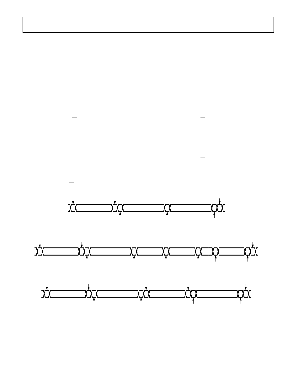
Figure 23 shows a typical write sequence for programming an
internal register. The cycle begins with a start condition, followed
by the hard coded 7-bit device address, which for the ADP5585
is 0x34, followed by the R/W bit set to 0 for a write cycle. The
ADP5585 acknowledges the address byte by pulling the data
line low. The address of the register to which data is to be written
is sent next. The ADP5585 acknowledges the register pointer
byte by pulling the data line low. The data byte to be written is
sent next. The ADP5585 acknowledges the data byte by pulling
the data line low. A stop condition completes the sequence.
Figure 24 shows a typical multibyte write sequence for program-
ming internal registers. The cycle begins with a start condition
followed by the 7-bit device address (0x34 for all models except
the ADP5585ACPZ-03-R7, 0x30 for the ADP5585ACPZ-03-R7
only), followed by the R/W bit set to 0 for a write cycle. The
ADP5585 acknowledges the address byte by pulling the data
line low. The address of the register to which data is to be written
is sent next. The ADP5585 acknowledges the register pointer
byte by pulling the data line low. The data byte to be written is
sent next. The ADP5585 acknowledges the data byte by pulling
the data line low. The pointer address is then incremented to
write the next data byte, until it finishes writing the n data byte.
The ADP5585 pulls the data line low after every byte, and a stop
condition completes the sequence.
Figure 25 shows a typical byte read sequence for reading inter-
nal registers. The cycle begins with a start condition followed
by the 7-bit device address (0x34 for all models except the
ADP5585ACPZ-03-R7, 0x30 for the ADP5585ACPZ-03-R7
only), followed by the R/W bit set to 0 for a write cycle. The
ADP5585 acknowledges the address byte by pulling the data line
low. The address of the register from which data is to be read is
sent next. The ADP5585 acknowledges the register pointer byte
by pulling the data line low. A start condition is repeated,
followed by the 7-bit device address (0x34 for all models except
the ADP5585ACPZ-03-R7, 0x30 for the ADP5585ACPZ-03-R7
only), followed by the R/W bit set to 1 for a read cycle. The
ADP5585 acknowledges the address byte by pulling the data
line low. The 8-bit data is then read. The host pulls the data line
high (no acknowledge), and a stop condition completes the
sequence.
START
0 = WRITE
7-BIT DEVICE ADDRESS
ADP5585 ACK
8-BIT REGISTER POINTER
8-BIT WRITE DATA
0
000
ADP5585 ACK
STOP
09
84
1-
02
2
Figure 23. I2C Single Byte Write Sequence
START
0 = WRITE
7-BIT DEVICE ADDRESS
ADP5585 ACK
8-BIT REGISTER POINTER
WRITE BYTE 1
WRITE BYTE 2
WRITE BYTE n
00
0
ADP5585 ACK
STOP
09
84
1-
02
3
Figure 24. I2C Multibyte Write Sequence
START
0 = WRITE
7-BIT DEVICE ADDRESS
ADP5585 ACK
8-BIT REGISTER POINTER
8-BIT READ DATA
00
0
1
0
1
REPEAT START
1 = READ
ADP5585 ACK
NO ACK
STOP
09
84
1-
02
4
Figure 25. I2C Single Byte Read Sequence
相關(guān)PDF資料 |
PDF描述 |
|---|---|
| EBM25DSEF-S13 | CONN EDGECARD 50POS .156 EXTEND |
| GSC06DRTH-S734 | CONN EDGECARD 12POS DIP .100 SLD |
| 5503995-4 | CABLE ASSEM FIBER ST-ST 5 METER |
| ADA4853-3YRU-EBZ | BOARD EVAL FOR ADA4853-3YRU |
| A3CCB-2636G | IDC CABLE- AKC26B/AE26G/AKC26B |
相關(guān)代理商/技術(shù)參數(shù) |
參數(shù)描述 |
|---|---|
| ADP5586 | 制造商:AD 制造商全稱(chēng):Analog Devices 功能描述:Keypad Decoder and I/O Port Expander |
| ADP5586ACBZ-00-R7 | 功能描述:接口-I/O擴(kuò)展器 RoHS:否 制造商:NXP Semiconductors 邏輯系列: 輸入/輸出端數(shù)量: 最大工作頻率:100 kHz 工作電源電壓:1.65 V to 5.5 V 工作溫度范圍:- 40 C to + 85 C 安裝風(fēng)格:SMD/SMT 封裝 / 箱體:HVQFN-16 封裝:Reel |
| ADP5586ACBZ-01-R7 | 功能描述:接口-I/O擴(kuò)展器 RoHS:否 制造商:NXP Semiconductors 邏輯系列: 輸入/輸出端數(shù)量: 最大工作頻率:100 kHz 工作電源電壓:1.65 V to 5.5 V 工作溫度范圍:- 40 C to + 85 C 安裝風(fēng)格:SMD/SMT 封裝 / 箱體:HVQFN-16 封裝:Reel |
| ADP5586ACBZ-03-R7 | 功能描述:接口-I/O擴(kuò)展器 RoHS:否 制造商:NXP Semiconductors 邏輯系列: 輸入/輸出端數(shù)量: 最大工作頻率:100 kHz 工作電源電壓:1.65 V to 5.5 V 工作溫度范圍:- 40 C to + 85 C 安裝風(fēng)格:SMD/SMT 封裝 / 箱體:HVQFN-16 封裝:Reel |
| ADP5586CB-EVALZ | 功能描述:界面開(kāi)發(fā)工具 RoHS:否 制造商:Bourns 產(chǎn)品:Evaluation Boards 類(lèi)型:RS-485 工具用于評(píng)估:ADM3485E 接口類(lèi)型:RS-485 工作電源電壓:3.3 V |
發(fā)布緊急采購(gòu),3分鐘左右您將得到回復(fù)。