- 您現(xiàn)在的位置:買賣IC網(wǎng) > PDF目錄374022 > ADP3522ACP-1.8 (ANALOG DEVICES INC) GSM Power Management System PDF資料下載
參數(shù)資料
| 型號(hào): | ADP3522ACP-1.8 |
| 廠商: | ANALOG DEVICES INC |
| 元件分類: | 電源管理 |
| 英文描述: | GSM Power Management System |
| 中文描述: | 1-CHANNEL POWER SUPPLY SUPPORT CKT, QCC32 |
| 封裝: | 5 X 5 MM, EXPOSED PAD, MO-220-VHHD-2, LFCSP-32 |
| 文件頁(yè)數(shù): | 12/20頁(yè) |
| 文件大小: | 467K |
| 代理商: | ADP3522ACP-1.8 |
第1頁(yè)第2頁(yè)第3頁(yè)第4頁(yè)第5頁(yè)第6頁(yè)第7頁(yè)第8頁(yè)第9頁(yè)第10頁(yè)第11頁(yè)當(dāng)前第12頁(yè)第13頁(yè)第14頁(yè)第15頁(yè)第16頁(yè)第17頁(yè)第18頁(yè)第19頁(yè)第20頁(yè)
REV. 0
–12–
ADP3522
SIMEN
VRTCIN
VRTC
BATSNS
MVBAT
CHRDET
CHRIN
SIMVSEL
NC
VAN
VBAT
VCORE
VMEM
VBAT2
VSIM
NC
N
R
P
P
T
A
R
V
GATEDR
G
D
I
E
C
R
R
PWRON
POWERKEY
ROWX
SIMEN
VRTC
CHRIN
MVBAT
CHRDET
SIMSEL
CLKON
REFOUT
VTCXO
VAN
VCORE
RESET
VMEM
VSIM
CHGEN
EOC
C3
10 F
C4
0.1 F
C5
2.2 F
C6
2.2 F
C7
2.2 F
C10
2.2 F
C8
0.1 F
C9
0.22 F
R8
10
Li OR NiMH
BATTERY
D1
BAT1000
Q1
SI3441
R1
0.25
COIN CELL
C1
0.1 F
C2
1nF
ADP3522
GATEIN
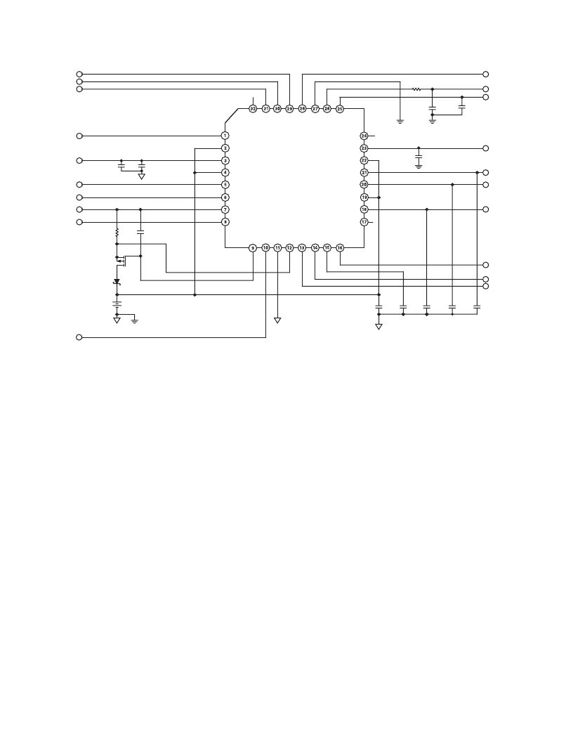
Figure 2.
Typical Application Circuit
THEORY OF OPERATION
The ADP3522 is a power management chip optimized for use
with GSM baseband chipsets in handset applications. Figure 1
shows a block diagram of the ADP3522. The ADP3522 con-
tains several blocks, such as:
Six low dropout regulators (SIM, core, analog, crystal
oscillator, memory, real-time clock)
Reset generator
Buffered precision reference
Lithium ion charge controller and processor interface
Power on/off logic
Undervoltage lockout
Deep discharge lockout
These functions have traditionally been done either as a discrete
implementation or as a custom ASIC design. The ADP3522
combines the benefits of both worlds by providing an integrated
standard product where every block is optimized to operate in a
GSM environment while maintaining a cost competitive solution.
Figure 2 shows the external circuitry associated with the
ADP3522. Only a minimal number of support components
are required.
Input Voltage
The input voltage range of the ADP3522 is 3 V to 5.5 V and is
optimized for a single Li-Ion cell or three NiMH cells. The type
of battery, the SIM LDO output voltage, and the memory LDO
output voltage will all affect the amount of power that the
ADP3522 needs to dissipate. The thermal impedance of the
CSP package is 32
°
C/W for a JEDEC standard 4-layer board.
The end of charge voltage for high capacity NiMH cells can be as
high as 5.5 V. This results in a worst-case power dissipation for
the ADP3522-1.8 to be as high as 1.6 W for NiMH cells. The
power dissipation for the ADP3522-3 is slightly lower at 1.45 W.
A fully charged Li-Ion battery is 4.25 V, where the ADP3522-3
can dissipate a maximum power of 0.85 W. However, the
ADP3522-1.8 can have a maximum dissipation of 1.0 W.
High battery voltages normally occur when the battery is being
charged and the handset is not in conversation mode. In this
mode, there is a relatively light load on the LDOs. The worst-
case power dissipation should be calculated based on the actual
load currents and voltages used.
Figure 3 shows the maximum power dissipation as a function of
the input voltage. Figure 4 shows the maximum allowable
power dissipation as a function of the ambient temperature.
Low Dropout Regulators (LDOs)
The ADP3522 high performance LDOs are optimized for their
given functions by balancing quiescent current, dropout voltage,
regulation, ripple rejection, and output noise. 2.2
μ
F tantalum
or MLCC ceramic capacitors are recommended for use with the
core, memory, SIM, and analog LDOs. A 0.22
μ
F capacitor is
recommended for the TCXO LDO.
相關(guān)PDF資料 |
PDF描述 |
|---|---|
| ADP3522ACP-3 | GSM Power Management System |
| ADP3604 | |
| ADP3604AR | Secondary Over-Voltage Protection for 2-4 cell in series Li-Ion/Poly (4.45V) 8-SM8 -40 to 110 |
| ADP3604* | Dual/Quad Rail-to-Rail Output, Picoamp Input Precision Op Amps; Package: SO; No of Pins: 8; Temperature Range: -40°C to +85°C |
| ADP3605ARU-3 | 120 mA Switched Capacitor Voltage Inverter with Regulated Output |
相關(guān)代理商/技術(shù)參數(shù) |
參數(shù)描述 |
|---|---|
| ADP3522ACP-3 | 制造商:AD 制造商全稱:Analog Devices 功能描述:GSM Power Management System |
| ADP3522ACP-3-REEL | 制造商:Analog Devices 功能描述:GSM Power Management System 32-Pin LFCSP EP T/R |
| ADP3522ACP-3-REEL7 | 制造商:Analog Devices 功能描述:GSM Power Management System 32-Pin LFCSP EP T/R 制造商:Rochester Electronics LLC 功能描述: |
| ADP35622901 | 制造商:LG Corporation 功能描述:Fan Assembly,Propeller |
發(fā)布緊急采購(gòu),3分鐘左右您將得到回復(fù)。