- 您現(xiàn)在的位置:買賣IC網(wǎng) > PDF目錄373968 > AD9807JS (ANALOG DEVICES INC) Complete 12-Bit/10-Bit 6 MSPS CCD/CIS Signal Processors PDF資料下載
參數(shù)資料
| 型號: | AD9807JS |
| 廠商: | ANALOG DEVICES INC |
| 元件分類: | 微控制器/微處理器 |
| 英文描述: | Complete 12-Bit/10-Bit 6 MSPS CCD/CIS Signal Processors |
| 中文描述: | SPECIALTY MICROPROCESSOR CIRCUIT, PQFP64 |
| 封裝: | PLASTIC, QFP-64 |
| 文件頁數(shù): | 20/24頁 |
| 文件大小: | 240K |
| 代理商: | AD9807JS |
AD9807/AD9805
–20–
REV. 0
NO
BRING STRTLN HIGH
THE FIRST PIXEL IS GREEN
THE SECOND PIXEL IS RED, ALTERNATING GRGR...
BRING STRTLN LOW AT THE END OF THE LINE
NEXT LINE
GRGR AGAIN
(NEW FRAME)
YES
APPLY AT LEAST ONE ADCCLK CYCLE
WRITE A "1" TO THE LSB OF THE BAYER REGISTER
BRING STRTLN LOW
SET PGA AND INPUT OFFSET FOR RED
PIXELS USING THE BLUE REGISTERS
SET PGA AND INPUT OFFSET FOR GREEN
PIXELS USING THE GREEN REGISTERS
CHANGE THE PGA AND INPUT OFFSET OF BLUE
REGISTERS FOR BLUE PIXELS
BRING STRTLN HIGH
THE FIRST PIXEL IS BLUE
THE SECOND PIXEL IS GREEN, ALTERNATING BGBG...
BRING STRTLN LOW AT THE END OF THE LINE
CHANGE GAIN
AND OFFSET
FOR RED PIXELS
WITH BLUE
REGISTERS
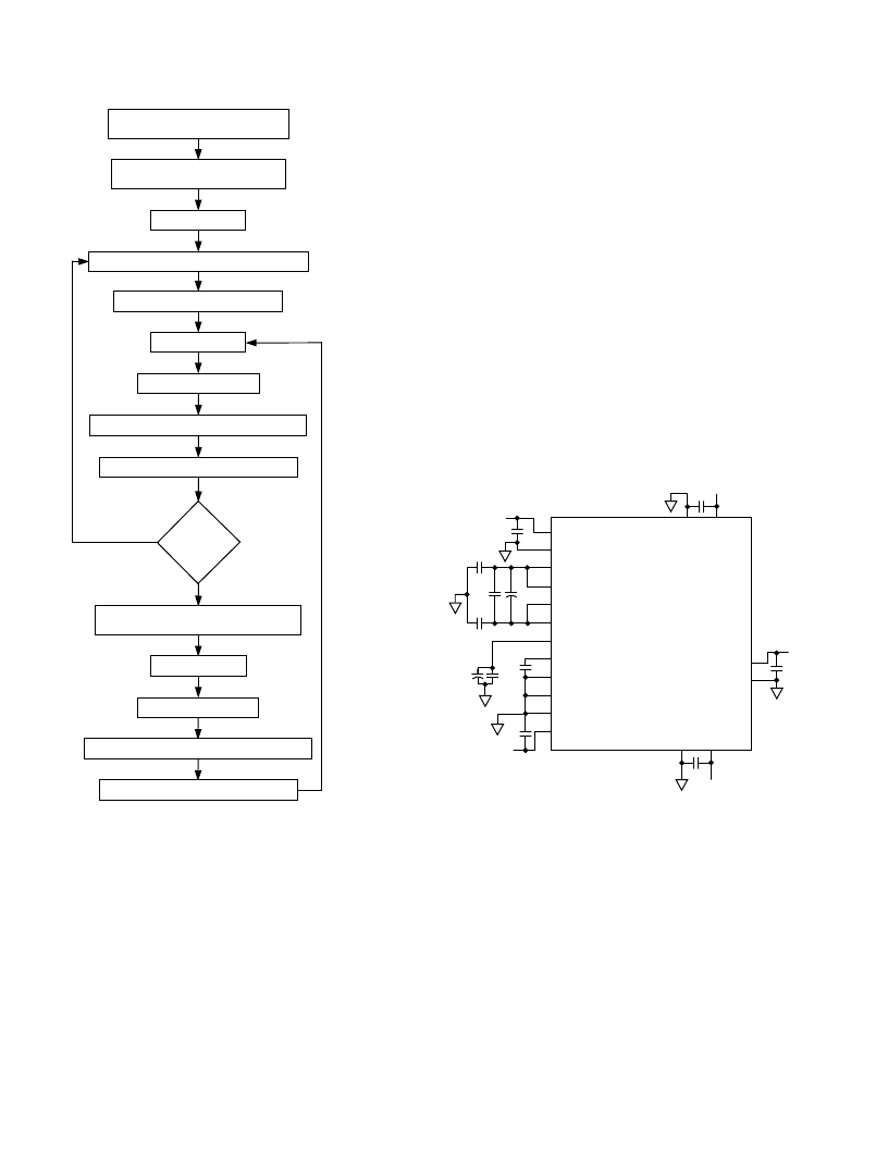
Figure 21. Bayer Mode Operation
Grounding and Decoupling
Figure 22 shows the recommended decoupling capacitors and
ground connections for the AD9807/AD9805. Notice that all of
the power and ground connections are common for the analog
and digital portions of the chip. T his would be the best way to
connect the device on a board containing a large number of
digital components. By treating the AD9807/AD9805 as an
analog component, the on-board digital circuitry is considered
“quiet digital” and the digital supply pins are connected to the
clean analog supply and analog ground plane. For this tech-
nique to work well, it is important that the digital supply pins be
well decoupled to the analog ground plane and that the digital
outputs of the AD9807/AD9805 are buffered to minimize the
digital drive current. T he buffers would be referred to the digital
supply and ground. T his scheme is preferable to tying the digital
portion of the AD9807/AD9805 to a noisy digital ground and
power plane, capacitively coupling noise to the analog circuitry
within the device. T he AD9807/AD9805 evaluation boards use
this grounding method, shown in Figures 26 and 27. If a
minimum amount of digital circuitry exists on the board, it is
possible that the power and ground connections of the AD9807
can be separated; be sure to maintain a single point connection
between the two ground planes at the AD9807/AD9805.
+5
0.1
μ
F
0.1
μ
F
0.1
μ
F
10
μ
F
+
0.1
μ
F
+
10
μ
F
0.1
μ
F
0.1
μ
F
0.1
μ
F
+5
52
DVSS
+5
0.1
μ
F
0.1
μ
F
+5
28
+5
0.1
μ
F
DVSS
DDVDD
29
41
40
51
1
AD9807/AD9805
(PINS OMITTED FOR CLARITY)
AVDD
AVSS
CAPT
CAPT
CAPB
CAPB
REF
CML
AVSS
AVSS
AVSS
AVDD
DRVDD
DRVSS
2
3
4
5
6
7
8
10
12
14
15
Figure 22.
相關(guān)PDF資料 |
PDF描述 |
|---|---|
| AD9806 | Complete 10-Bit 18 MSPS CCD Signal Processor |
| AD9806KST | Complete 10-Bit 18 MSPS CCD Signal Processor |
| AD9814 | LABELS,CABLE MARKERS,CABLE MARKERS,LABELS, CABLE MARKERS,WIRE IDENTIFICATION AND MARKING SYSTEMS,SHRINK TUBING LABELS ,KROY RoHS Compliant: NA |
| AD9814JR | LABELS,CABLE MARKERS,CABLE MARKERS,LABELS, CABLE MARKERS,WIRE IDENTIFICATION AND MARKING SYSTEMS,SHRINK TUBING LABELS ,KROY RoHS Compliant: NA |
| AD9814KR | Complete 14-Bit CCD/CIS Signal Processor |
相關(guān)代理商/技術(shù)參數(shù) |
參數(shù)描述 |
|---|---|
| AD9808AJST | 制造商:Rochester Electronics LLC 功能描述:- Tape and Reel |
| AD9808AJSTRL | 制造商:Rochester Electronics LLC 功能描述:- Tape and Reel |
| AD9808JST | 制造商:Rochester Electronics LLC 功能描述:- Tape and Reel |
| AD9808JSTRL | 制造商:Rochester Electronics LLC 功能描述:- Tape and Reel |
| AD9812JR | 制造商:Analog Devices 功能描述: |
發(fā)布緊急采購,3分鐘左右您將得到回復(fù)。