- 您現(xiàn)在的位置:買賣IC網(wǎng) > PDF目錄373968 > AD9807JS (ANALOG DEVICES INC) Complete 12-Bit/10-Bit 6 MSPS CCD/CIS Signal Processors PDF資料下載
參數(shù)資料
| 型號: | AD9807JS |
| 廠商: | ANALOG DEVICES INC |
| 元件分類: | 微控制器/微處理器 |
| 英文描述: | Complete 12-Bit/10-Bit 6 MSPS CCD/CIS Signal Processors |
| 中文描述: | SPECIALTY MICROPROCESSOR CIRCUIT, PQFP64 |
| 封裝: | PLASTIC, QFP-64 |
| 文件頁數(shù): | 15/24頁 |
| 文件大?。?/td> | 240K |
| 代理商: | AD9807JS |
AD9807/AD9805
–15–
REV. 0
R (n–2)
G (n–2)
B (n–2)
R (n–1)
G (n–1)
B (n–1)
R (n)
PIXEL n
PIXEL n+1
PIXEL n+2
R, G, B
R, G, B
R, G, B
R
G
B
R
G
B
R
G
B
RIN, GIN, BIN
CDSCLK1
CDSCLK2
ADCCLK
DATA<11:0>
G (n+1)
B (n+1)
R (n+2)
G (n+2)
B (n+2)
R (n+3)
GAIN<n:0>
GAIN<m:0>
R (n)
G (n)
B (n)
R (n+1)
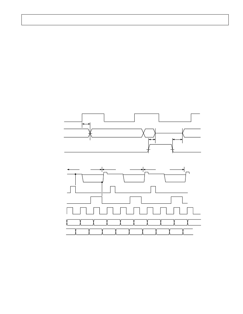
Figure 12. DOUT Latency, 3-Channel CDS Mode
t
OD
t
HZ
t
EDV
ADCCLK
DATA<11:0>
OEB
Figure 11. Digital Output Timing
is inverted and amplified by the PGA; the setting in the corre-
sponding PGA Gain Register determines the gain of the PGA.
T he output from the PGA is then routed through a high speed
multiplexer to a 12-bit A/D converter (10-bit for AD9805) for
digitization; the multiplexer does cycle in this mode. After
digitization, the data is modified by the amount indicated in
the Even Offset Registers. A digital subtracter allows additional
pixel rate offset modification of the signal based on the values
written to the OFFSET data bus. Finally, a digital multiplier
allows pixel rate gain modification of the signal based on the
values written to the GAIN data bus. Latency is 6 ADCCL K
cycles (7 cycles for the gain and offset bus; see Figure 14).
T he state of ST RT L N is evaluated on the rising edges of
ADCCLK . When ST RT LN is low, the internal circuitry is
reset on the next rising edge of ADCCL K ; the odd/even
circuitry is configured to expect even pixels.
T his feature has been included to accommodate the use of the
part with an area CCD (Bayer Mode). T he mode is initiated by
writing a one to the LSB of the register at Address 7 (see Figure
21). T he write to enable the mode should be performed when
the ST RT LN input is inactive (low) and the ADCCLK is running.
T he first pixel after an active edge on ST RT LN will be a green
pixel. All pixels in Bayer Mode are even and use the even offset
registers. T he line will continue alternating GRGRGR pixels
until ST RT LN goes inactive. T he next line will be BGBGBG
pixels (the first pixel after the active ST RT LN edge being blue).
Line type will then alternate between GRGRGR and BGBGBG
type. T o reset the next line to GRGRGR type at the start of the
next frame/image, rewrite the Bayer mode enable bit to a one
during the inactive ST RT L N period. All red and blue pixels
pass through the blue channel of the part and use the blue PGA
and offset registers. T o use a different offset/PGA gain value the
register must be written to between lines. Green pixels on either
line type pass through the green channel.
相關(guān)PDF資料 |
PDF描述 |
|---|---|
| AD9806 | Complete 10-Bit 18 MSPS CCD Signal Processor |
| AD9806KST | Complete 10-Bit 18 MSPS CCD Signal Processor |
| AD9814 | LABELS,CABLE MARKERS,CABLE MARKERS,LABELS, CABLE MARKERS,WIRE IDENTIFICATION AND MARKING SYSTEMS,SHRINK TUBING LABELS ,KROY RoHS Compliant: NA |
| AD9814JR | LABELS,CABLE MARKERS,CABLE MARKERS,LABELS, CABLE MARKERS,WIRE IDENTIFICATION AND MARKING SYSTEMS,SHRINK TUBING LABELS ,KROY RoHS Compliant: NA |
| AD9814KR | Complete 14-Bit CCD/CIS Signal Processor |
相關(guān)代理商/技術(shù)參數(shù) |
參數(shù)描述 |
|---|---|
| AD9808AJST | 制造商:Rochester Electronics LLC 功能描述:- Tape and Reel |
| AD9808AJSTRL | 制造商:Rochester Electronics LLC 功能描述:- Tape and Reel |
| AD9808JST | 制造商:Rochester Electronics LLC 功能描述:- Tape and Reel |
| AD9808JSTRL | 制造商:Rochester Electronics LLC 功能描述:- Tape and Reel |
| AD9812JR | 制造商:Analog Devices 功能描述: |
發(fā)布緊急采購,3分鐘左右您將得到回復(fù)。