- 您現(xiàn)在的位置:買賣IC網(wǎng) > PDF目錄17059 > AD9737A-EBZ (Analog Devices Inc)BOARD EVAL FOR AD9737A PDF資料下載
參數(shù)資料
| 型號: | AD9737A-EBZ |
| 廠商: | Analog Devices Inc |
| 文件頁數(shù): | 53/64頁 |
| 文件大?。?/td> | 0K |
| 描述: | BOARD EVAL FOR AD9737A |
| 標準包裝: | 1 |
| 系列: | * |
第1頁第2頁第3頁第4頁第5頁第6頁第7頁第8頁第9頁第10頁第11頁第12頁第13頁第14頁第15頁第16頁第17頁第18頁第19頁第20頁第21頁第22頁第23頁第24頁第25頁第26頁第27頁第28頁第29頁第30頁第31頁第32頁第33頁第34頁第35頁第36頁第37頁第38頁第39頁第40頁第41頁第42頁第43頁第44頁第45頁第46頁第47頁第48頁第49頁第50頁第51頁第52頁當前第53頁第54頁第55頁第56頁第57頁第58頁第59頁第60頁第61頁第62頁第63頁第64頁

Data Sheet
AD9737A/AD9739A
Rev. | Page 57 of 64
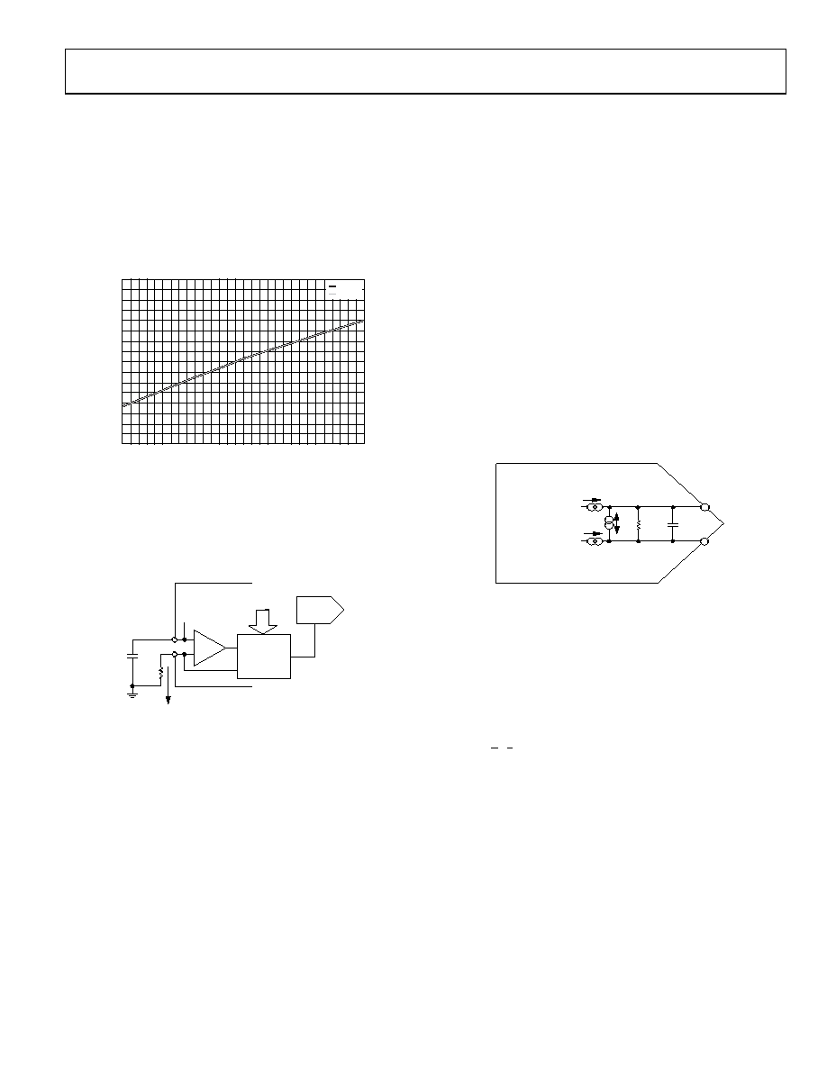
The AD9737A/AD9739A clock receiver features the ability to
independently adjust the common-mode level of its inputs over
a span of ±100 mV centered about its mid-supply point (that is,
VDDC/2), as well as an offset for hysteresis purposes. Figure 175
shows the equivalent input circuit of one of the inputs. ESD
diodes are not shown for clarity purposes. It has been found
through characterization that the optimum setting is for both
inputs to be biased at approximately 0.8 V. This can be achieved
by writing a 0x0F (corresponding to a 15) setting to both cross
controller registers (that is, Register 0x22 and Register 0x23).
0.70
0.75
0.80
0.85
0.90
0.95
1.00
1.05
1.10
–15 –13 –11
–9
–7
–5
–3
–1
1
3
5
7
9
11
13
15
OFFSET CODE
C
O
MMO
N
MO
D
E
(V)
CLKP
CLKN
09616-
095
Figure 176. Common-Mode Voltage with Respect to
CLKP_OFFSET/CLKN_OFFSET and DIR_P/DIR_N
VOLTAGE REFERENCE
The AD9737A/AD9739A output current is set by a combination
of digital control bits and the I120 reference current, as shown
CURRENT
SCALING
FSC[9:0]
AD9737A/AD9739A
DAC
IFULL-SCALE
10k
1nF
VREF
I120
VSSA
I120
VBG
1.2V
+
–
09616-
096
Figure 177. Voltage Reference Circuit
The reference current is obtained by forcing the band gap voltage
across an external 10 k resistor from I120 (Pin B14) to ground.
The 1.2 V nominal band gap voltage (VREF) generates a 120 A
reference current in the 10 k resistor. Note the following
constraints when configuring the voltage reference circuit:
Both the 10 k resistor and 1 nF bypass capacitor are required
for proper operation.
Digitally adjust the DAC’s output full-scale current, IOUTFS,
from its default setting of 20 mA.
Modulating the reference current, I120, with an ac signal is
not supported.
The band gap voltage appearing at the VREF pin (Pin C14)
must be buffered for use with an external circuitry because
its output impedance is approximately 5 k.
An external reference can be used to overdrive the internal
reference by connecting it to the VREF pin.
IOUTFS can be adjusted digitally over 8.7 mA to 31.7 mA by using
FSC[9:0] (Register 0x06 and Register 0x07).
The following equation relates IOUTFS to the FSC[9:0] bits, which
can be set from 0 to 1023.
IOUTFS = 22.6 × FSC[9:0]/1000 + 8.7
(1)
Note that a default value of 0x200 generates 20 mA full scale, which
is used for most of the characterization presented in this data
sheet (unless noted otherwise).
ANALOG OUTPUTS
Equivalent DAC Output and Transfer Function
The AD9737A/AD9739A provide complementary current
outputs, IOUTP and IOUTN, that source current into an external
ground reference load. Figure 178 shows an equivalent output
circuit for the DAC. Note that, compared to most current output
slight offset current (that is, IOUTFS/16), and the peak differential
ac current is slightly below IOUTFS/2 (that is, 15/32 × IOUTFS).
17/32 × IOUTFS
IPEAK =
15/32 × IOUTFS
AC
70
2.2pF
IOUTFS = 8.6 – 31.2mA
17/32 × IOUTFS
09616-
097
Figure 178. Equivalent DAC Output Circuit
As shown in Figure 178, the DAC output can be modeled as a
pair of dc current sources that source a current of 17/32 × IOUTFS to
each output. A differential ac current source, IPEAK, is used to
model the signal-dependent nature of the DAC output. The
polarity and signal dependency of this ac current source are
related to the digital code by the following equation:
F(Code) = (DACCODE 8192)/8192
(2)
1 < F(Code) < 1
(3)
where DACCODE = 0 to 16,383 (decimal).
Because IPEAK can swing ±(15/32) × IOUTFS, the output currents
measured at IOUTP and IOUTN can span from IOUTFS/16 to IOUTFS.
However, because the ac signal-dependent current component
is complementary, the sum of the two outputs is always constant
(that is, IOUTP + IOUTN = (34/32) × IOUTFS).
C
相關(guān)PDF資料 |
PDF描述 |
|---|---|
| MIC2026-1YM | IC DISTRIBUTION SW DUAL 8-SOIC |
| VI-B1L-EY | CONVERTER MOD DC/DC 28V 50W |
| AD9706-DPG2-EBZ | BOARD EVAL FOR AD9706 |
| AD9705-DPG2-EBZ | BOARD EVAL FOR AD9705 |
| MIC2026-2YM | IC DISTRIBUTION SW DUAL 8-SOIC |
相關(guān)代理商/技術(shù)參數(shù) |
參數(shù)描述 |
|---|---|
| AD9739 | 制造商:AD 制造商全稱:Analog Devices 功能描述:14-Bit, 2.5 GSPS, RF Digital-to-Analog Converter |
| AD9739A | 制造商:AD 制造商全稱:Analog Devices 功能描述:14-Bit, 2.5 GSPS, RF Digital-to-Analog Converter |
| AD9739ABBC | 制造商:Analog Devices 功能描述:14 BIT 2.5 GSPS DAC A REVISION - Trays |
| AD9739ABBCRL | 制造商:Analog Devices 功能描述:14 BIT 2.5 GSPS DAC A REVISION - Tape and Reel |
| AD9739ABBCZ | 功能描述:數(shù)模轉(zhuǎn)換器- DAC 14 Bit 2.5 GSPS DAC A Revision RoHS:否 制造商:Texas Instruments 轉(zhuǎn)換器數(shù)量:1 DAC 輸出端數(shù)量:1 轉(zhuǎn)換速率:2 MSPs 分辨率:16 bit 接口類型:QSPI, SPI, Serial (3-Wire, Microwire) 穩(wěn)定時間:1 us 最大工作溫度:+ 85 C 安裝風格:SMD/SMT 封裝 / 箱體:SOIC-14 封裝:Tube |
發(fā)布緊急采購,3分鐘左右您將得到回復。