- 您現(xiàn)在的位置:買賣IC網(wǎng) > PDF目錄373893 > AD7225UQ (ANALOG DEVICES INC) LC2MOS Quad 8-Bit DAC with Separate Reference Inputs PDF資料下載
參數(shù)資料
| 型號(hào): | AD7225UQ |
| 廠商: | ANALOG DEVICES INC |
| 元件分類: | DAC |
| 英文描述: | LC2MOS Quad 8-Bit DAC with Separate Reference Inputs |
| 中文描述: | QUAD, PARALLEL, 8 BITS INPUT LOADING, 8-BIT DAC, CDIP24 |
| 封裝: | CERDIP-24 |
| 文件頁(yè)數(shù): | 9/12頁(yè) |
| 文件大小: | 339K |
| 代理商: | AD7225UQ |
AD7225
REV. B
–9–
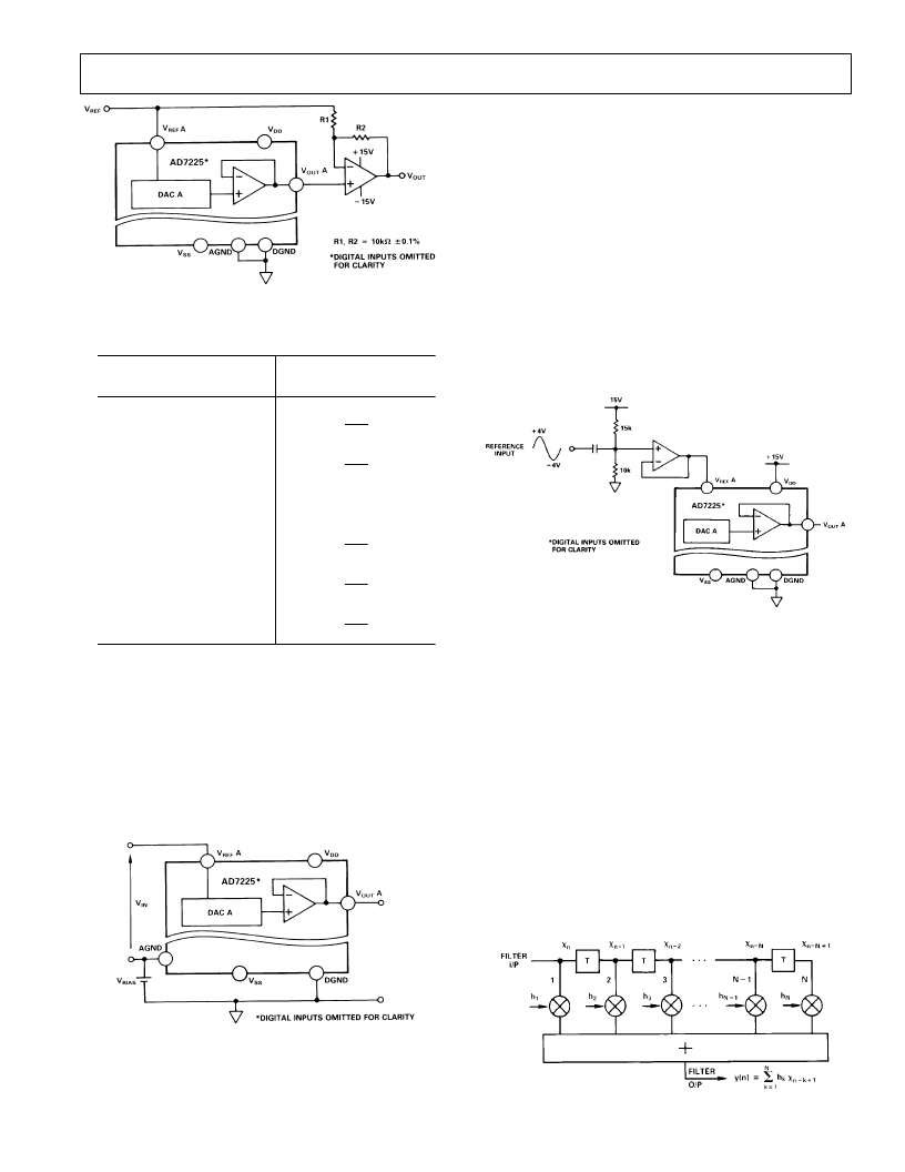
Figure 14. AD7225 Bipolar Output Circuit
T able IV. Bipolar (Offset Binary) Code T able
DAC Latch Contents
MSB
LSB
Analog Output
1 1 1 1
1 1 1 1
+
V
REF
127
128
1 0 0 0
0 0 0 1
+
V
REF
1
128
1 0 0 0
0 0 0 0
0 V
0 1 1 1
1 1 1 1
±
V
REF
1
128
0 0 0 0
0 0 0 1
±
V
REF
127
128
0 0 0 0
0 0 0 0
±
V
REF
128
128
±
V
REF
AGND BIAS
T he AD7225 AGND pin can be biased above system GND
(AD7225 DGND) to provide an offset “zero” analog output
voltage level. Figure 15 shows a circuit configuration to achieve
this for channel A of the AD7225. T he output voltage, V
OUT
A,
can be expressed as:
V
OUT
A
=
V
BIAS
+
D
A
(
V
IN
)
where
D
A
is a fractional representation of the digital word in
DAC latch A. (0
≤
D
A
≤
255/256).
Figure 15. AGND Bias Circuit
For a given V
IN
, increasing AGND above system GND will re-
duce the effective V
DD
–V
REF
which must be at least 4 V to en-
sure specified operation. Note that because the AGND pin is
common to all four DACs, this method biases up the output
voltages of all the DACs in the AD7225. Note that V
DD
and V
SS
of the AD7225 should be referenced to DGND.
AC RE FE RE NCE SIGNAL
In some applications it may be desirable to have ac reference
signals. T he AD7225 has multiplying capability within the up-
per (V
DD
– 4 V) and lower (2 V) limits of reference voltage when
operated with dual supplies. T herefore ac signals need to be ac
coupled and biased up before being applied to the reference in-
puts. Figure 16 shows a sine wave signal applied to V
REF
A. For
input signal frequencies up to 50 kHz the output distortion typi-
cally remains less than 0.1%. T he typical 3 dB bandwidth figure
for small signal inputs is 800 kHz.
Figure 16. Applying an AC Signal to the AD7225
APPLIC AT IONS
PROGRAMMABLE T RANSVE RSAL FILT E R
A discrete-time filter may be described by either multiplication
in the frequency domain or convolution in the time domain i.e.
Y
ω
( )
=
H
ω
( )
X
ω
( )
or
y
n
= ∑
T he convolution sum may be implemented using the special
structure known as the transversal filter (Figure 17). Basically, it
consists of an N-stage delay line with N taps weighted by N co-
efficients, the resulting products being accumulated to form the
output. T he tap weights or coefficients h
k
are actually the non-
zero elements of the impulse response and therefore determine
the filter transfer function. A particular filter frequency response
is realized by setting the coefficients to the appropriate values.
T his property leads to the implementation of transversal filters
whose frequency response is programmable.
=
1
N
h
kX n
±
k
+
1
Figure 17. Transversal Filter
相關(guān)PDF資料 |
PDF描述 |
|---|---|
| AD7225KN | LC2MOS Quad 8-Bit DAC with Separate Reference Inputs |
| AD7225KP | LC2MOS Quad 8-Bit DAC with Separate Reference Inputs |
| AD7225KR | LC2MOS Quad 8-Bit DAC with Separate Reference Inputs |
| AD7225TE | LC2MOS Quad 8-Bit DAC with Separate Reference Inputs |
| AD7225TQ | LC2MOS Quad 8-Bit DAC with Separate Reference Inputs |
相關(guān)代理商/技術(shù)參數(shù) |
參數(shù)描述 |
|---|---|
| AD7225UQ/883B | 制造商:未知廠家 制造商全稱:未知廠家 功能描述:8-Bit Digital-to-Analog Converter |
| AD7226 | 制造商:AD 制造商全稱:Analog Devices 功能描述:LC2MOS Quad 8-Bit D/A Converter |
| AD7226B/D | 制造商:未知廠家 制造商全稱:未知廠家 功能描述:8-Bit Digital-to-Analog Converter |
| AD7226BCHIPS | 制造商:未知廠家 制造商全稱:未知廠家 功能描述:8-Bit Digital-to-Analog Converter |
| AD7226BE | 制造商:Rochester Electronics LLC 功能描述:- Bulk |
發(fā)布緊急采購(gòu),3分鐘左右您將得到回復(fù)。