- 您現(xiàn)在的位置:買賣IC網(wǎng) > PDF目錄373886 > AD6122ACPRL (ANALOG DEVICES INC) CDMA 3 V Transmitter IF Subsystem with Integrated Voltage Regulator PDF資料下載
參數(shù)資料
| 型號: | AD6122ACPRL |
| 廠商: | ANALOG DEVICES INC |
| 元件分類: | 通信及網(wǎng)絡(luò) |
| 英文描述: | CDMA 3 V Transmitter IF Subsystem with Integrated Voltage Regulator |
| 中文描述: | SPECIALTY TELECOM CIRCUIT, PQCC32 |
| 封裝: | MO-220-VHHD-2, LPCC-32 |
| 文件頁數(shù): | 11/20頁 |
| 文件大?。?/td> | 264K |
| 代理商: | AD6122ACPRL |
REV. B
AD6122
–
11
–
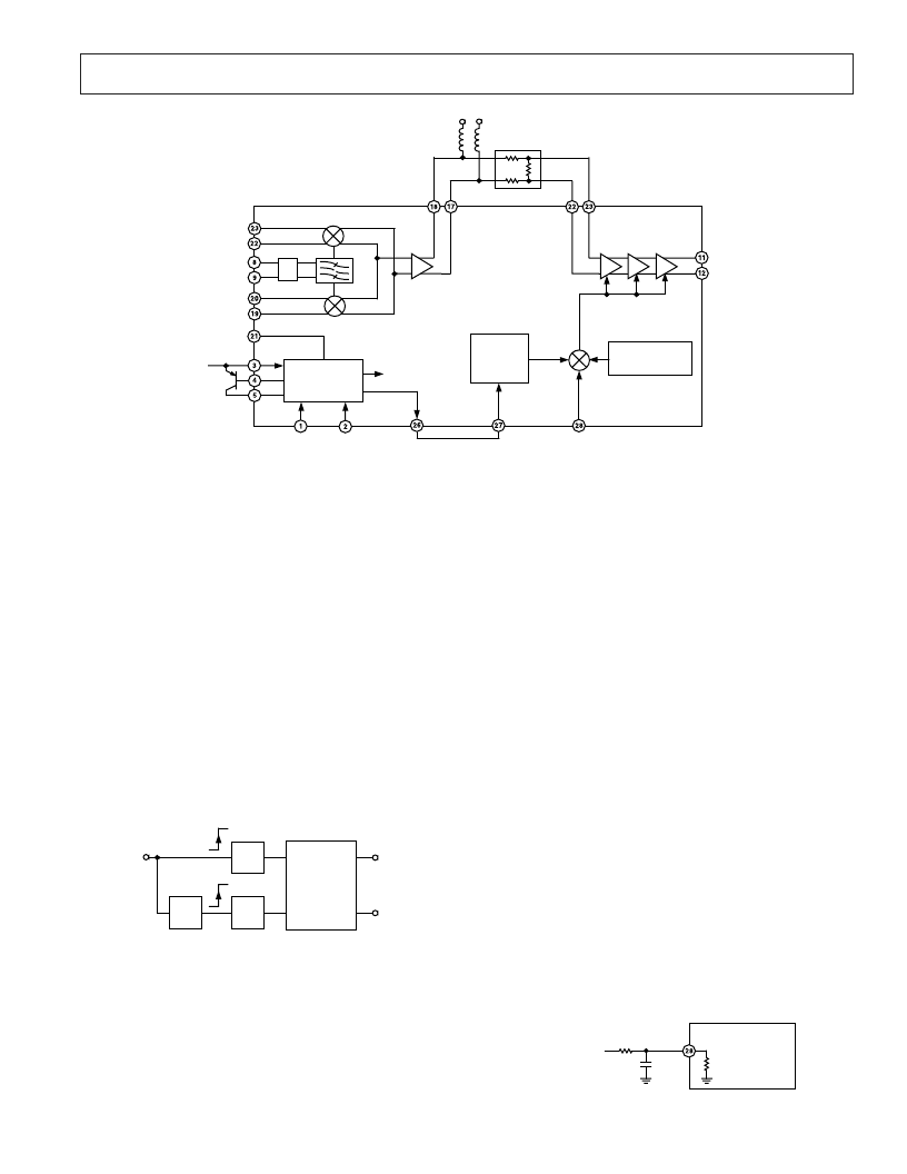
THEORY OF OPERATION
The CDMA Transmitter IF Subsystem (Figure 21) consists of
an I and Q modulator with a divide-by-two quadrature genera-
tor, high dynamic range IF amplifiers with voltage-controlled
gain, a low dropout regulator and power-down control inputs.
I and Q Modulator
The I and Q modulator accepts differential quadrature baseband
inputs from CDMA baseband converters. The LO is injected at
twice the IF frequency. A divide-by-two quadrature generator
followed by dual polyphase filters ensures
±
1
°
quadrature accu-
racy (Figure 22).
For 500 mV p-p differential I and Q input signals, the output
power of the modulator will be –21 dBm referred to 1 k
when
the output of the modulator is loaded with a 1 k
differential
load. With the maximum input conditions stated above, the
modulator outputs are a 225
μ
A p-p differential current; conse-
quently, the output load will greatly affect the output power of
the modulator.
2
180
2
POLYPHASE
FILTERS
I
Q
I
Q
2 IF
LO INPUT
QUADRATURE
OUTPUT TO
MODULATOR
Figure 22. Simplified Quadrature Generator Circuit
The I and Q modulator also provides a common mode reference
signal at the MODCMREF pin. This voltage is a dc voltage set
to 1.408 V when a 2.7 V supply is used. It is used to dc bias
the output of the DAC that provides I and Q inputs to the
modulator.
IF Amplifiers and Gain Control
The IF amplifiers provide an 86 dB linear in dB gain control
range. The input stage uses a differential, continuously variable
attenuator based on Analog Devices’ patented X-AMP topol-
ogy. This low noise attenuator consists of a differential R-2R
ladder network, linear interpolator and a fixed gain amplifier.
The IF amplifier’s input impedance is 1 k
differential. Similar
to the I and Q modulator’s output, the IF amplifier’s output is a
differential current, which will vary depending upon the gain
control voltage. In order to achieve the specified gain, the out-
put of the IF amplifiers should be loaded with a 1 k
differen-
tial load.
The gain control circuits contain both temperature compensa-
tion circuitry and a choice of internal or external reference for
adjusting the gain scale factor. The gain control input accepts
an external gain control voltage input from a DAC. It provides
97 dB of gain control range with a nominal 75 dB/V scale factor.
The external gain control input signal should be a clean signal.
It is recommended to filter this signal in order to eliminate the
noise that results from the DAC. If a noisy signal is used for the
gain control voltage, VGAIN inband and adjacent channel noise
peaking can occur at the output of the AD6122. A simple RC
filter can be employed, but care should be taken with its design.
If too big a resistor is used, a large voltage drop may occur
across the resistor, resulting in lower gain than expected (as a
result of a lower voltage reaching the AD6122). An RC filter
with a 20 kHz bandwidth, employing a 1 k
resistor is appropri-
ate. This results in an 8.2 nF capacitor. The resulting circuit
is shown in Figure 23. Note that the input resistance at the
VGAIN pin is approximately 100 k
.
FROM
BASEBAND
CONVERTER
AD6122
VGAIN
109k
1k
8.2nF
Figure 23. Gain Voltage Filtering
I INPUT
Q INPUT
LOCAL
OSCILLATOR
INPUT
ATTENUATOR
COMMON-MODE
REFERENCE
OUTPUT
VREG
POWER-
DOWN 1
1.23 V
REFERENCE
OUTPUT
VPOS
TEMPERATURE
COMPENSATION
GAIN CONTROL
VOLTAGE
INPUT
GAIN CONTROL
REFERENCE
VOLTAGE
INPUT
TRANSMIT
OUTPUT
IF AMPLIFIERS
QUADRATURE MODULATOR
VCC
POWER-
DOWN 2
IF AMPLIFIER
INPUT
QUADRATURE
MODULATOR
OUTPUT
2
AD6122
GAIN
CONTROL
SCALE
FACTOR
LOW
DROPOUT
REGULATOR
Figure 21. Block Diagram
X-AMP is a trademark of Analog Devices, Inc.
相關(guān)PDF資料 |
PDF描述 |
|---|---|
| AD6122 | CDMA 3 V Receiver IF Subsystem with Integrated Voltage Regulator(低功耗接收中頻子系統(tǒng)) |
| AD6140ARSRL | Bandpass IF Subsystem |
| AD6140ARS | RE Series - Econoline Unregulated DC-DC Converters; Input Voltage (Vdc): 3.3V; Output Voltage (Vdc): 12V; Power: 1W; Industry Standard Pinout; 1kVDC & 2kVDC Isolation; UL94V-0 Package Material; Optional Continuous Short Circuit Protected; Fully Encapsulated; Custom Solutions Available; Efficiency to 85% |
| AD6140 | Bandpass ∑△ IF Subsystem(帶通∑△IF子系統(tǒng)) |
| AD6190ARSRL | 900 MHz RF Transceiver |
相關(guān)代理商/技術(shù)參數(shù) |
參數(shù)描述 |
|---|---|
| AD6122ARS | 制造商:AD 制造商全稱:Analog Devices 功能描述:CDMA 3 V Transmitter IF Subsystem with Integrated Voltage Regulator |
| AD6122ARSRL | 制造商:AD 制造商全稱:Analog Devices 功能描述:CDMA 3 V Transmitter IF Subsystem with Integrated Voltage Regulator |
| AD612BS | 制造商:POP 功能描述: |
| AD6140 | 制造商:AD 制造商全稱:Analog Devices 功能描述:Bandpass IF Subsystem |
| AD6140ARS | 制造商:Rochester Electronics LLC 功能描述:- Bulk |
發(fā)布緊急采購,3分鐘左右您將得到回復(fù)。