- 您現(xiàn)在的位置:買賣IC網 > PDF目錄373886 > AD6122ACPRL (ANALOG DEVICES INC) CDMA 3 V Transmitter IF Subsystem with Integrated Voltage Regulator PDF資料下載
參數(shù)資料
| 型號: | AD6122ACPRL |
| 廠商: | ANALOG DEVICES INC |
| 元件分類: | 通信及網絡 |
| 英文描述: | CDMA 3 V Transmitter IF Subsystem with Integrated Voltage Regulator |
| 中文描述: | SPECIALTY TELECOM CIRCUIT, PQCC32 |
| 封裝: | MO-220-VHHD-2, LPCC-32 |
| 文件頁數(shù): | 1/20頁 |
| 文件大小: | 264K |
| 代理商: | AD6122ACPRL |
REV. B
Information furnished by Analog Devices is believed to be accurate and
reliable. However, no responsibility is assumed by Analog Devices for its
use, nor for any infringements of patents or other rights of third parties
which may result from its use. No license is granted by implication or
otherwise under any patent or patent rights of Analog Devices.
a
AD6122
One Technology Way, P.O. Box 9106, Norwood, MA 02062-9106, U.S.A.
Tel: 781/329-4700
World Wide Web Site: http://www.analog.com
Fax: 781/326-8703
Analog Devices, Inc., 2000
CDMA 3 V Transmitter IF Subsystem
with Integrated Voltage Regulator
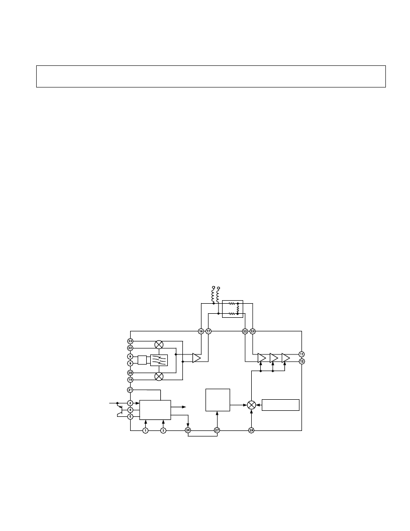
FUNCTIONAL BLOCK DIAGRAM
I INPUT
Q INPUT
LOCAL
OSCILLATOR
INPUT
ATTENUATOR
LOW
DROPOUT
REGULATOR
COMMON-MODE
REFERENCE
OUTPUT
VREG
POWER-
DOWN 1
1.23 V
REFERENCE
OUTPUT
VPOS
TEMPERATURE
COMPENSATION
GAIN
CONTROL
SCALE
FACTOR
GAIN CONTROL
VOLTAGE
INPUT
GAIN CONTROL
REFERENCE
VOLTAGE
INPUT
TRANSMIT
OUTPUT
IF AMPLIFIERS
QUADRATURE MODULATOR
POWER-
DOWN 2
IF AMPLIFIER
INPUT
QUADRATURE
MODULATOR
OUTPUT
2
AD6122
VCC
FEATURES
Fully Compliant with IS98A and PCS Specifications
Linear IF Amplifier
–63 dB to +34 dB
Linear-in-dB Gain Control
Temperature-Compensated Gain Control
Quadrature Modulator
Modulates IFs from 50 MHz to 350 MHz
Integral Low Dropout Regulator
Accepts 2.9 V to 4.2 V Input from Battery
Low Power
10.4 mA at Midgain
<10 A Sleep Mode Operation
Companion Receiver IF Chip Available (AD6121)
APPLICATIONS
CDMA, W-CDMA, AMPS and TACS Operation
QPSK Transmitters
GENERAL DESCRIPTION
The AD6122 is a low power IF transmitter subsystem, specifi-
cally designed for CDMA applications. It consists of an I and Q
modulator, a divide-by-two quadrature generator, high dynamic
range IF amplifiers with voltage-controlled gain and a power-
down control input. An integral low dropout regulator allows
operation from battery voltages from 2.9 V to 4.2 V.
The gain control input accepts an external gain control voltage
input from a DAC. It provides 97 dB of gain control with a
nominal 75 dB/V scale factor. Either an internal or an external
reference may be used to set the gain-control scale factor.
The I and Q modulator accepts differential quadrature base-
band inputs from a CDMA baseband converter. The local oscil-
lator is injected at twice the IF frequency. A divide-by-two
quadrature generator followed by dual polyphase filters ensures
±
1
°
quadrature accuracy.
The modulator provides a common-mode reference output to
bias the transmit DACs in the baseband converter to the same
common-mode voltage as the modulator inputs, allowing dc
coupling between the two ICs and thus eliminating the need to
charge and discharge coupling capacitors. This allows the fastest
power-up and power-down times for the AD6122 and CDMA
baseband ICs.
The AD6122 is fabricated using a 25 GHz f
t
silicon BiCMOS
process and is packaged in a 28-lead SSOP and a 32-leadless
LPCC chip scale package (5 mm
×
5 mm).
相關PDF資料 |
PDF描述 |
|---|---|
| AD6122 | CDMA 3 V Receiver IF Subsystem with Integrated Voltage Regulator(低功耗接收中頻子系統(tǒng)) |
| AD6140ARSRL | Bandpass IF Subsystem |
| AD6140ARS | RE Series - Econoline Unregulated DC-DC Converters; Input Voltage (Vdc): 3.3V; Output Voltage (Vdc): 12V; Power: 1W; Industry Standard Pinout; 1kVDC & 2kVDC Isolation; UL94V-0 Package Material; Optional Continuous Short Circuit Protected; Fully Encapsulated; Custom Solutions Available; Efficiency to 85% |
| AD6140 | Bandpass ∑△ IF Subsystem(帶通∑△IF子系統(tǒng)) |
| AD6190ARSRL | 900 MHz RF Transceiver |
相關代理商/技術參數(shù) |
參數(shù)描述 |
|---|---|
| AD6122ARS | 制造商:AD 制造商全稱:Analog Devices 功能描述:CDMA 3 V Transmitter IF Subsystem with Integrated Voltage Regulator |
| AD6122ARSRL | 制造商:AD 制造商全稱:Analog Devices 功能描述:CDMA 3 V Transmitter IF Subsystem with Integrated Voltage Regulator |
| AD612BS | 制造商:POP 功能描述: |
| AD6140 | 制造商:AD 制造商全稱:Analog Devices 功能描述:Bandpass IF Subsystem |
| AD6140ARS | 制造商:Rochester Electronics LLC 功能描述:- Bulk |
發(fā)布緊急采購,3分鐘左右您將得到回復。