- 您現(xiàn)在的位置:買賣IC網(wǎng) > PDF目錄373859 > AD1837AAS (ANALOG DEVICES INC) 2 ADC, 8 DAC, 96 kHz, 24-Bit Codec PDF資料下載
參數(shù)資料
| 型號: | AD1837AAS |
| 廠商: | ANALOG DEVICES INC |
| 元件分類: | 消費家電 |
| 英文描述: | 2 ADC, 8 DAC, 96 kHz, 24-Bit Codec |
| 中文描述: | SPECIALTY CONSUMER CIRCUIT, PQFP52 |
| 封裝: | PLASTIC, MS-022AC, MQFP-52 |
| 文件頁數(shù): | 12/24頁 |
| 文件大小: | 401K |
| 代理商: | AD1837AAS |
REV. A
AD1837A
–12–
DAC ENGINE
CLOCK SCALING
1
2
2/3
MCLK
DAC INPUT
INTERPOLATION
FILTER
-
MODULATOR
DAC
48kHz/96kHz/192kHz
ADC ENGINE
ADC OUTPUT
OPTIONAL
HPF
DECIMATOR/
FILTER
48kHz/96kHz
ANALOG
OUTPUT
ANALOG
INPUT
12.288MHz
IMCLK = 24.576MHz
-
MODULATOR
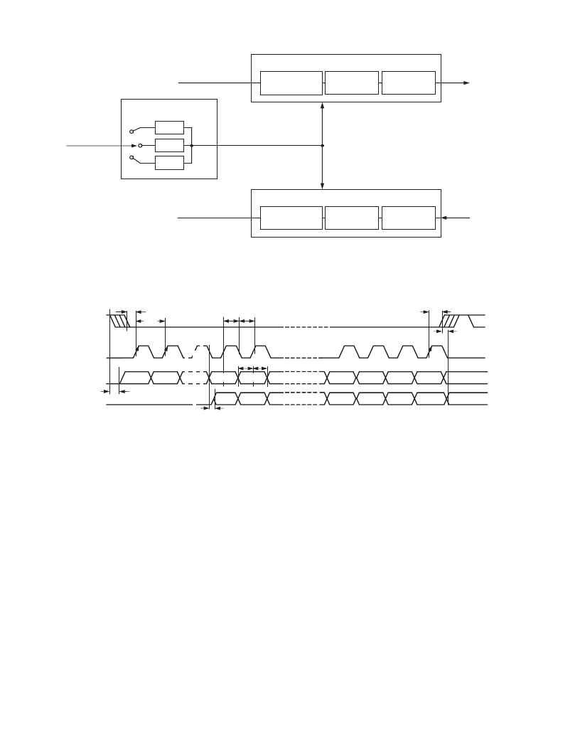
Figure 2. Modulator Clocking Scheme
CLATCH
CCLK
CIN
COUT
D0
D8
D0
D15
D14
D9
D8
t
CCH
t
CCL
D9
t
CDS
t
CDH
t
CLS
t
CLH
t
COD
t
COTS
t
CCP
t
COE
Figure 3. Format of SPI Timing
DAC outputs if the jitter spectrum contains large spectral peaks.
It is highly recommended that the master clock be generated by
an independent crystal oscillator. In addition, it is especially
important that the clock signal not be passed through an FPGA
or other large digital chip before being applied to the AD1837A.
In most cases, this will induce clock jitter due to the fact that
the clock signal is sharing common power and ground connec-
tions with other unrelated digital output signals.
Power-Down and RESET
PD
/
RST
powers down the chip and sets the control registers to
their default settings. After
PD
/
RST
is de-asserted, an initialization
routine runs inside the AD1837A to clear all memories to zero.
This initialization lasts for approximately 20 LRCLK intervals.
During this time, it is recommended that no SPI writes occur.
Power Supply and Voltage Reference
The AD1837A is designed for 5 V supplies. Separate power
supply pins are provided for the analog and digital sections.
These pins should be bypassed with 100 nF ceramic chip capaci-
tors, as close to the pins as possible, to minimize noise pickup. A
bulk aluminum electrolytic capacitor of at least 22
m
F should also
be
provided on the same PC board as the codec. For critical appli-
cations, improved performance will be obtained with separate sup-
plies for the analog and digital sections. If this is not possible, it is
recommended that the analog and digital supplies be isolated by
means of two ferrite beads in series with the bypass capacitor of
each supply. It is important that the analog supply be as clean
as possible.
The internal voltage reference is brought out on the FILTR pin
and should be bypassed as close as possible to the chip, with a
parallel combination of 10
m
F and 100 nF. The reference voltage
may be used to bias external op amps to the common-mode
voltage of the analog input and output signal pins. The current
drawn from the V
REF
pin should be limited to less than 50
m
A.
Serial Control Port
The AD1837A has an SPI compatible control port to permit
programming the internal control registers for the ADCs and
DACs and for reading the ADC signal levels from the internal
peak detectors. The SPI control port is a 4-wire serial control port.
The format is similar to the Motorola SPI format except the
input data-word is 16 bits wide. The maximum serial bit clock
frequency is 12.5 MHz and may be completely asynchronous to
the sample rate of the ADCs and DACs. Figure 3 shows the
format of the SPI signal.
Serial Data Ports—Data Format
The ADC serial data output mode defaults to the popular I
2
S
format, where the data is delayed by one BCLK interval from
the edge of the LRCLK. By changing Bits 6 to 8 in ADC
相關(guān)PDF資料 |
PDF描述 |
|---|---|
| AD1837AAS-REEL | 2 ADC, 8 DAC, 96 kHz, 24-Bit Codec |
| AD1837AASZ-REEL | 2 ADC, 8 DAC, 96 kHz, 24-Bit Codec |
| AD1837 | 2 ADC, 8 DAC, 96 kHz, 24-Bit Codec |
| AD1837AS | 2 ADC, 8 DAC, 96 kHz, 24-Bit Codec |
| AD1837AS-REEL | 2 ADC, 8 DAC, 96 kHz, 24-Bit Codec |
相關(guān)代理商/技術(shù)參數(shù) |
參數(shù)描述 |
|---|---|
| AD1837AAS-REEL | 制造商:AD 制造商全稱:Analog Devices 功能描述:2 ADC, 8 DAC, 96 kHz, 24-Bit Codec |
| AD1837AASZ | 制造商:Analog Devices 功能描述:Audio Codec 2ADC / 8DAC 24-Bit 52-Pin MQFP 制造商:Analog Devices 功能描述:IC CODEC SMD 1837 MQFP52 |
| AD1837AASZ-REEL | 制造商:Analog Devices 功能描述:Audio Codec 2ADC / 8DAC 24-Bit 52-Pin MQFP T/R |
| AD1837AS | 制造商:Analog Devices 功能描述:Audio Codec 2ADC / 8DAC 24-Bit 52-Pin MQFP 制造商:Rochester Electronics LLC 功能描述:- Bulk |
| AD1837AS-REEL | 制造商:Analog Devices 功能描述:Audio Codec 2ADC / 8DAC 24-Bit 52-Pin MQFP T/R |
發(fā)布緊急采購,3分鐘左右您將得到回復(fù)。