- 您現(xiàn)在的位置:買賣IC網(wǎng) > PDF目錄352477 > A42MX16-2BG100A (Electronic Theatre Controls, Inc.) 40MX and 42MX FPGA Families PDF資料下載
參數(shù)資料
| 型號(hào): | A42MX16-2BG100A |
| 廠商: | Electronic Theatre Controls, Inc. |
| 英文描述: | 40MX and 42MX FPGA Families |
| 中文描述: | 40MX和42MX FPGA系列 |
| 文件頁(yè)數(shù): | 98/120頁(yè) |
| 文件大?。?/td> | 854K |
| 代理商: | A42MX16-2BG100A |
第1頁(yè)第2頁(yè)第3頁(yè)第4頁(yè)第5頁(yè)第6頁(yè)第7頁(yè)第8頁(yè)第9頁(yè)第10頁(yè)第11頁(yè)第12頁(yè)第13頁(yè)第14頁(yè)第15頁(yè)第16頁(yè)第17頁(yè)第18頁(yè)第19頁(yè)第20頁(yè)第21頁(yè)第22頁(yè)第23頁(yè)第24頁(yè)第25頁(yè)第26頁(yè)第27頁(yè)第28頁(yè)第29頁(yè)第30頁(yè)第31頁(yè)第32頁(yè)第33頁(yè)第34頁(yè)第35頁(yè)第36頁(yè)第37頁(yè)第38頁(yè)第39頁(yè)第40頁(yè)第41頁(yè)第42頁(yè)第43頁(yè)第44頁(yè)第45頁(yè)第46頁(yè)第47頁(yè)第48頁(yè)第49頁(yè)第50頁(yè)第51頁(yè)第52頁(yè)第53頁(yè)第54頁(yè)第55頁(yè)第56頁(yè)第57頁(yè)第58頁(yè)第59頁(yè)第60頁(yè)第61頁(yè)第62頁(yè)第63頁(yè)第64頁(yè)第65頁(yè)第66頁(yè)第67頁(yè)第68頁(yè)第69頁(yè)第70頁(yè)第71頁(yè)第72頁(yè)第73頁(yè)第74頁(yè)第75頁(yè)第76頁(yè)第77頁(yè)第78頁(yè)第79頁(yè)第80頁(yè)第81頁(yè)第82頁(yè)第83頁(yè)第84頁(yè)第85頁(yè)第86頁(yè)第87頁(yè)第88頁(yè)第89頁(yè)第90頁(yè)第91頁(yè)第92頁(yè)第93頁(yè)第94頁(yè)第95頁(yè)第96頁(yè)第97頁(yè)當(dāng)前第98頁(yè)第99頁(yè)第100頁(yè)第101頁(yè)第102頁(yè)第103頁(yè)第104頁(yè)第105頁(yè)第106頁(yè)第107頁(yè)第108頁(yè)第109頁(yè)第110頁(yè)第111頁(yè)第112頁(yè)第113頁(yè)第114頁(yè)第115頁(yè)第116頁(yè)第117頁(yè)第118頁(yè)第119頁(yè)第120頁(yè)
79
4958B–AUTO–11/10
Atmel ATA6285/ATA6286 [Preliminary]
Bit 0 - T0F: Timer0 Flag Bit
When the interval timer in Timer0 generates an output clock pulse (CLK
T0) the T0F bit is set
(one). If the I-bit in SREG and the T0IE bit is set (one) at T0CR the MCU will jump to the corre-
sponding Interrupt Vector. The flag is cleared when the interrupt routine is executed.
Alternatively, the flag can be cleared by writing a logical one to it.
3.13.4
Timer1
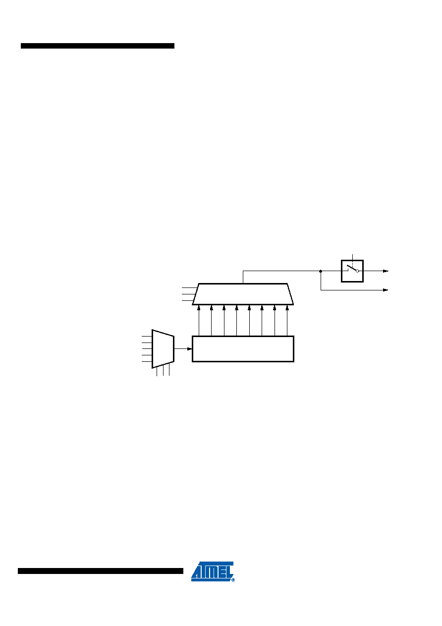
The Timer1 is an interval timer which can be used to generate periodical interrupts and as pres-
caler for Timer2, and Timer3. The Timer1 consists of a programmable 12-bit divider that input
clock (CL1) can be driven by the Timer0 output clock (CLK
T0), I/O clock (CLKI/O), Timer clock
(CLT), the external input clock (T2I) and the external input clock (T3I). The three bits T1CS[2..0]
select the input clock (CL1) for Timer1. The timer output signal can be used as prescaler clock
and as source for the Timer1 interrupt. The interrupt is maskable via the T1IE bit and also the
time interval for the timer output can be adjusted as shown in Figure 3-28 via the T1PS[2..0] bits
in the Timer1 control register T1CR. The timer interrupt flag bit (T1F) is located in the T10IFR
register.
Figure 3-28. Timer1 Block Diagram
T1PS2
T1PS1
T1PS0
CL1
INTT0
12-bit Prescaler
Input
MUX
Output MUX-Timer1
TC1/256
TC1/16
TC1/2
T1C
S
0
T1C
S
1
T1C
S
2
TC1/4
TC1/
8
TC1/
3
2
TC1/1K
TC1/4K
T1IE
CLKT0
CLKI/O
T3I
T2I
CLT
CLKT1
相關(guān)PDF資料 |
PDF描述 |
|---|---|
| A42MX24-2BG100A | 40MX and 42MX FPGA Families |
| A42MX36-2BG100A | 40MX and 42MX FPGA Families |
| A42MX02-2BG100B | 40MX and 42MX FPGA Families |
| A42MX04-2BG100B | 40MX and 42MX FPGA Families |
| A42MX09-2BG100B | 40MX and 42MX FPGA Families |
相關(guān)代理商/技術(shù)參數(shù) |
參數(shù)描述 |
|---|---|
| A42MX16-2BG100B | 制造商:未知廠家 制造商全稱:未知廠家 功能描述:40MX and 42MX FPGA Families |
| A42MX16-2BG100ES | 制造商:未知廠家 制造商全稱:未知廠家 功能描述:40MX and 42MX FPGA Families |
| A42MX16-2BG100I | 制造商:未知廠家 制造商全稱:未知廠家 功能描述:40MX and 42MX FPGA Families |
| A42MX16-2BG100M | 制造商:未知廠家 制造商全稱:未知廠家 功能描述:40MX and 42MX FPGA Families |
| A42MX16-2CQ100 | 制造商:未知廠家 制造商全稱:未知廠家 功能描述:40MX and 42MX FPGA Families |
發(fā)布緊急采購(gòu),3分鐘左右您將得到回復(fù)。