- 您現(xiàn)在的位置:買賣IC網(wǎng) > PDF目錄36339 > 935273916557 (NXP SEMICONDUCTORS) COLOR SIGNAL DECODER, PBGA156 PDF資料下載
參數(shù)資料
| 型號: | 935273916557 |
| 廠商: | NXP SEMICONDUCTORS |
| 元件分類: | 顏色信號轉(zhuǎn)換 |
| 英文描述: | COLOR SIGNAL DECODER, PBGA156 |
| 封裝: | 15 X 15 MM, 1.15 MM HEIGHT, PLASTIC, MS-034, SOT-472-1, BGA-156 |
| 文件頁數(shù): | 123/178頁 |
| 文件大小: | 988K |
| 代理商: | 935273916557 |
第1頁第2頁第3頁第4頁第5頁第6頁第7頁第8頁第9頁第10頁第11頁第12頁第13頁第14頁第15頁第16頁第17頁第18頁第19頁第20頁第21頁第22頁第23頁第24頁第25頁第26頁第27頁第28頁第29頁第30頁第31頁第32頁第33頁第34頁第35頁第36頁第37頁第38頁第39頁第40頁第41頁第42頁第43頁第44頁第45頁第46頁第47頁第48頁第49頁第50頁第51頁第52頁第53頁第54頁第55頁第56頁第57頁第58頁第59頁第60頁第61頁第62頁第63頁第64頁第65頁第66頁第67頁第68頁第69頁第70頁第71頁第72頁第73頁第74頁第75頁第76頁第77頁第78頁第79頁第80頁第81頁第82頁第83頁第84頁第85頁第86頁第87頁第88頁第89頁第90頁第91頁第92頁第93頁第94頁第95頁第96頁第97頁第98頁第99頁第100頁第101頁第102頁第103頁第104頁第105頁第106頁第107頁第108頁第109頁第110頁第111頁第112頁第113頁第114頁第115頁第116頁第117頁第118頁第119頁第120頁第121頁第122頁當前第123頁第124頁第125頁第126頁第127頁第128頁第129頁第130頁第131頁第132頁第133頁第134頁第135頁第136頁第137頁第138頁第139頁第140頁第141頁第142頁第143頁第144頁第145頁第146頁第147頁第148頁第149頁第150頁第151頁第152頁第153頁第154頁第155頁第156頁第157頁第158頁第159頁第160頁第161頁第162頁第163頁第164頁第165頁第166頁第167頁第168頁第169頁第170頁第171頁第172頁第173頁第174頁第175頁第176頁第177頁第178頁
2004 Jul 22
49
Philips Semiconductors
Product specication
Multistandard video decoder with adaptive
comb lter and component video input
SAA7118
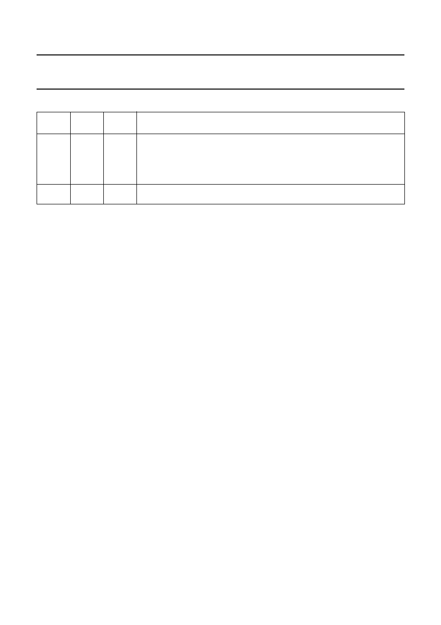
Table 9
Processing trigger and start
XDV1
92H[5]
XDV0
92H[4]
XDH
92H[2]
DESCRIPTION
Internal decoder: The processing triggers at the falling edge of the V123 pulse
decoder HREF at line number:
0
1
0
4/7 (50/60 Hz, 1st field), respectively 3/6 (50/60 Hz, 2nd field) (decoder count)
0
2/5 (50/60 Hz, 1st field), respectively 2/5 (50/60 Hz, 2nd field) (decoder count)
000
External ITU 656 stream: The processing starts earliest with SAV at line number 23
(50 Hz system), respectively line 20 (60 Hz system) (according to ITU 656 count)
8.4.1.2
Task handling
The task handler controls the switching between the two
programming register sets. It is controlled by
subaddresses 90H and C0H. A task is enabled via the
global control bits TEA[80H[4]] and TEB[80H[5]].
The handler is then triggered by events, which can be
defined for each register set.
In the event of a programming error the task handling and
the complete scaler can be reset to the initial states by
setting the software reset bit SWRST[88H[5]] to logic 0.
Especially if the programming registers, related acquisition
window and scale are reprogrammed while a task is active,
a software reset must be performed after programming.
Contrary to the disabling/enabling of a task, which is
evaluated at the end of a running task, when SWRST is at
logic 0 it sets the internal state machines directly to their
idle states.
The start condition for the handler is defined by bits
STRC[1:0] 90H[1:0] and means: start immediately, wait for
next V-sync, next FID at logic 0 or next FID at logic 1. The
FID is evaluated, if the vertical and horizontal offsets are
reached.
When RPTSK[90H[2]] is at logic 1 the actual running task
is repeated (under the defined trigger conditions), before
handing control over to the alternate task.
To support field rate reduction, the handler is also enabled
to skip fields (bits FSKP[2:0] 90H[5:3]) before executing
the task. A TOGGLE flag is generated (used for the correct
output field processing), which changes state at the
beginning of a task, every time a task is activated;
examples are given in Section 8.4.1.3.
Remarks:
To activate a task the start condition must be
fulfilled and the acquisition window offsets must be
reached.
For example, in case of ‘start immediately’, and two
regions are defined for one field, the offset of the lower
region must be greater than (offset + length) of the
upper region, if not, the actual counted H and V position
at the end of the upper task is beyond the programmed
offsets and the processing will ‘wait for next V’.
Basically the trigger conditions are checked, when a
task is activated. It is important to realize, that they are
not checked while a task is inactive. So you can not
trigger to next logic 0 or logic 1 with overlapping offset
and active video ranges between the tasks (e.g. task A
STRC[2:0] = 2, YO[11:0] = 310 and task B
STRC[2:0] = 3, YO[11:0] = 310 results in output field
rate of 50
3 Hz).
After power-on or software reset (via
SWRST[88H[5]]) task B gets priority over task A.
8.4.1.3
Output eld processing
As a reference for the output field processing, two signals
are available for the back-end hardware.
These signals are the input field ID from the scaler source
and a TOGGLE flag, which shows that an active task is
used an odd (1, 3, 5...) or even (2, 4, 6...) number of times.
Using a single or both tasks and reducing the field or frame
rate with the task handling function, the TOGGLE
information can be used to reconstruct an interlaced
scaled picture at a reduced frame rate. The TOGGLE flag
isn’t synchronized to the input field detection, as it is only
dependent on the interpretation of this information by the
external hardware, whether the output of the scaler is
processed correctly; see Section 8.4.3.
相關(guān)PDF資料 |
PDF描述 |
|---|---|
| 935268460118 | 1-CHANNEL, SGL POLE SGL THROW SWITCH, PDSO5 |
| 935268459115 | 1-CHANNEL, SGL POLE SGL THROW SWITCH, PDSO5 |
| 935268459118 | 1-CHANNEL, SGL POLE SGL THROW SWITCH, PDSO5 |
| 935268459125 | 1-CHANNEL, SGL POLE SGL THROW SWITCH, PDSO5 |
| 935268459165 | 1-CHANNEL, SGL POLE SGL THROW SWITCH, PDSO5 |
相關(guān)代理商/技術(shù)參數(shù) |
參數(shù)描述 |
|---|---|
| 935275527134 | 制造商:NXP Semiconductors 功能描述:IC BUS SWITCH OCTAL QUAD 20TSSOP |
| 935277864112 | 制造商:NXP Semiconductors 功能描述:IC CPU |
| 935278818112 | 制造商:NXP Semiconductors 功能描述:LCD DRVR 20DIGIT 2.5V/3.3V/5V 56-Pin VSO Tube |
| 935280517132 | 制造商:NXP Semiconductors 功能描述:IC TRANSLATING BUFFER 6XSON |
| 935281751112 | 制造商:NXP Semiconductors 功能描述:IC BUFFER/DVR 16BIT 3ST 48TSSOP |
發(fā)布緊急采購,3分鐘左右您將得到回復。