- 您現(xiàn)在的位置:買賣IC網(wǎng) > PDF目錄68813 > 73S8010C-IM/F (MAXIM INTEGRATED PRODUCTS INC) SPECIALTY ANALOG CIRCUIT, QCC32 PDF資料下載
參數(shù)資料
| 型號(hào): | 73S8010C-IM/F |
| 廠商: | MAXIM INTEGRATED PRODUCTS INC |
| 元件分類: | 模擬信號(hào)調(diào)理 |
| 英文描述: | SPECIALTY ANALOG CIRCUIT, QCC32 |
| 封裝: | 5 X 5 MM, LEAD FREE, QFN-32 |
| 文件頁(yè)數(shù): | 25/27頁(yè) |
| 文件大?。?/td> | 348K |
| 代理商: | 73S8010C-IM/F |
第1頁(yè)第2頁(yè)第3頁(yè)第4頁(yè)第5頁(yè)第6頁(yè)第7頁(yè)第8頁(yè)第9頁(yè)第10頁(yè)第11頁(yè)第12頁(yè)第13頁(yè)第14頁(yè)第15頁(yè)第16頁(yè)第17頁(yè)第18頁(yè)第19頁(yè)第20頁(yè)第21頁(yè)第22頁(yè)第23頁(yè)第24頁(yè)當(dāng)前第25頁(yè)第26頁(yè)第27頁(yè)
DS_8010C_024
73S8010C Data Sheet
Rev. 1.5
7
2
Host Interface (I
2C Bus)
A fast-mode 400 kHz I
2C bus slave interface is used for controlling the device and reading the status of
the device via the data pin SDA and clock pin SCL. The bus has 3 address select pins, SAD0, SAD1,
and SAD2. This allows up to 8 devices to be connected in parallel.
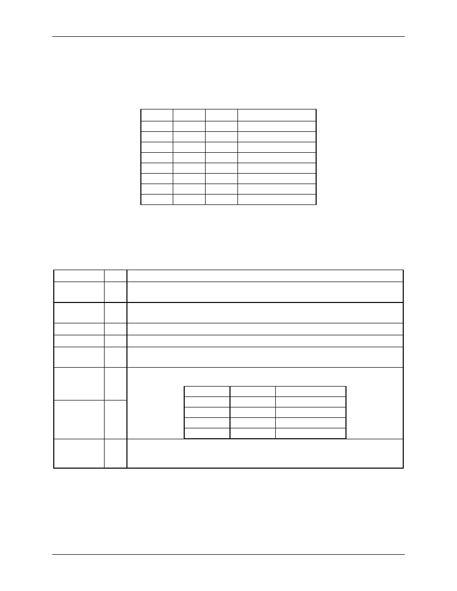
Table 1: Device Address Selections
SAD2
SAD1
SAD0
I
2C Address (7 bits)
0
0x40
0
1
0x42
0
1
0
0x44
0
1
0x46
1
0
0x48
1
0
1
0x4A
1
0
0x4C
1
0x4E
Bit 0 of the I
2C address is the R/W bit. Refer to Figure 2 and Figure 3 for usage.
2.1
Host Interface Control
Table 2 describes the Host Interface Control Register bits (power-on Reset = 0x00).
Table 2: Host Control Register
Name
Bit
Description
Start/Stop
0
When set, initiates an activation and a cold reset procedure; when reset, initiates
a deactivation sequence.
Warm reset
1
When set, initiates a warm reset procedure; automatically reset by hardware
when the card starts answering or when the card is declared mute.
5 V and 3 V
2
When set, VCC = 3 V; when reset, VCC = 5 V.
Clock Stop
3
When set, card clock is stopped. Bit 4 determines the card clock stop level.
Clock Stop
Level
4
When set, card clock stops high; when reset card clock stops low.
Clksel1
5
Bits 5 and 6 determine the clock rate to the card according to the following table.
CLKDIV1
CLKDIV2
Clock Rate
0
XTALIN/8
0
1
XTALIN/4
1
XTALIN/2
1
0
XTALIN
Clksel2
6
I/O enable
7
When set, data is transferred between I/O (AUX1, AUX2) and I/OUC (AUX1UC,
AUX2UC); when reset, I/O (AUX1, AUX2) and I/OUC (AUX1UC, AUX2UC) are
high impedance.
I
2C-bus Write to the Control Register
The I
2C-bus Write command to the control register follows the format shown in Figure 2.
After the START condition, the master sends a slave address. This address is seven bits long followed
by an eighth bit, which is an opcode bit (R/W) – a ‘zero’ indicates the master will write data to the control
register. After the R/W bit, the ’zero’ ACK bit is sent to the master by the device. The master now starts
sending the 8 bits of data to the control register during the DATA bits time. After the DATA bits, the ‘zero’
相關(guān)PDF資料 |
PDF描述 |
|---|---|
| 73S8010C-IL | SPECIALTY ANALOG CIRCUIT, PDSO28 |
| 73S8010C-IMR | SPECIALTY ANALOG CIRCUIT, QCC32 |
| 73S8010C-IL | SPECIALTY ANALOG CIRCUIT, PDSO28 |
| 73S8010C-IM | SPECIALTY ANALOG CIRCUIT, QCC32 |
| 73S8010C-IM | SPECIALTY ANALOG CIRCUIT, QCC32 |
相關(guān)代理商/技術(shù)參數(shù) |
參數(shù)描述 |
|---|---|
| 73S8010C-IMR/F | 功能描述:I2C 接口集成電路 Smart Card Interface ISO7816-3 & EVM4.0 RoHS:否 制造商:NXP Semiconductors 電源電壓-最大:5.5 V 電源電壓-最小:2.3 V 最大工作頻率:400 KHz 最大工作溫度:+ 85 C 封裝 / 箱體:TSSOP-16 |
| 73S8010C-IMR/F1 | 功能描述:I2C 接口集成電路 RoHS:否 制造商:NXP Semiconductors 電源電壓-最大:5.5 V 電源電壓-最小:2.3 V 最大工作頻率:400 KHz 最大工作溫度:+ 85 C 封裝 / 箱體:TSSOP-16 |
| 73S8010C-IMR/F2 | 功能描述:I2C 接口集成電路 RoHS:否 制造商:NXP Semiconductors 電源電壓-最大:5.5 V 電源電壓-最小:2.3 V 最大工作頻率:400 KHz 最大工作溫度:+ 85 C 封裝 / 箱體:TSSOP-16 |
| 73S8010R | 制造商:TERIDIAN 制造商全稱:TERIDIAN 功能描述:Low Cost Smart Card Interface |
| 73S8010R-DB | 功能描述:界面開發(fā)工具 73S8010R Demo Brd RoHS:否 制造商:Bourns 產(chǎn)品:Evaluation Boards 類型:RS-485 工具用于評(píng)估:ADM3485E 接口類型:RS-485 工作電源電壓:3.3 V |
發(fā)布緊急采購(gòu),3分鐘左右您將得到回復(fù)。