- 您現(xiàn)在的位置:買賣IC網(wǎng) > PDF目錄379075 > CY7C1472V33-200BZC (CYPRESS SEMICONDUCTOR CORP) 72-Mbit (2M x 36/4M x 18/1M x 72) Pipelined SRAM with NoBL Architecture PDF資料下載
參數(shù)資料
| 型號(hào): | CY7C1472V33-200BZC |
| 廠商: | CYPRESS SEMICONDUCTOR CORP |
| 元件分類: | DRAM |
| 英文描述: | 72-Mbit (2M x 36/4M x 18/1M x 72) Pipelined SRAM with NoBL Architecture |
| 中文描述: | 4M X 18 ZBT SRAM, 3 ns, PBGA165 |
| 封裝: | 15 X 17 MM, 1.40 MM HEIGHT, FBGA-165 |
| 文件頁(yè)數(shù): | 21/28頁(yè) |
| 文件大小: | 378K |
| 代理商: | CY7C1472V33-200BZC |
第1頁(yè)第2頁(yè)第3頁(yè)第4頁(yè)第5頁(yè)第6頁(yè)第7頁(yè)第8頁(yè)第9頁(yè)第10頁(yè)第11頁(yè)第12頁(yè)第13頁(yè)第14頁(yè)第15頁(yè)第16頁(yè)第17頁(yè)第18頁(yè)第19頁(yè)第20頁(yè)當(dāng)前第21頁(yè)第22頁(yè)第23頁(yè)第24頁(yè)第25頁(yè)第26頁(yè)第27頁(yè)第28頁(yè)
PRELIMINARY
CY7C1470V33
CY7C1472V33
CY7C1474V33
Document #: 38-05289 Rev. *E
Page 21 of 28
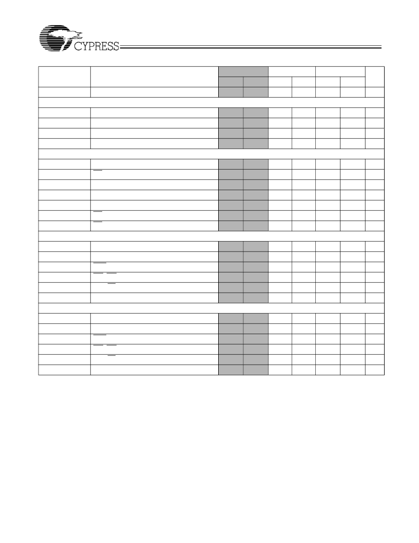
Switching Characteristics
Over the Operating Range
[16, 17]
Parameter
t
Power[18]
Clock
t
CYC
F
MAX
t
CH
t
CL
Output Times
t
CO
t
OEV
t
DOH
t
CHZ
t
CLZ
t
EOHZ
t
EOLZ
Set-up Times
t
AS
t
DS
t
CENS
t
WES
t
ALS
t
CES
Hold Times
t
AH
t
DH
t
CENH
t
WEH
t
ALH
t
CEH
Shaded areas contain advance information.
Description
-250
-200
-167
Unit
ms
Min.
1
Max.
Min.
1
Max.
Min.
1
Max.
V
CC
(typical) to the First Access Read or Write
Clock Cycle Time
Maximum Operating Frequency
Clock HIGH
Clock LOW
4.0
5.0
6.0
ns
MHz
ns
ns
250
200
167
2.0
2.0
2.0
2.0
2.2
2.2
Data Output Valid After CLK Rise
OE LOW to Output Valid
Data Output Hold After CLK Rise
Clock to High-Z
[19, 20, 21]
Clock to Low-Z
[19, 20, 21]
OE HIGH to Output High-Z
[19, 20, 21]
OE LOW to Output Low-Z
[19, 20, 21]
3.0
3.0
3.0
3.0
3.4
3.4
ns
ns
ns
ns
ns
ns
ns
1.3
1.3
1.5
3.0
3.0
3.4
1.3
1.3
1.5
3.0
3.0
3.4
0
0
0
Address Set-up Before CLK Rise
Data Input Set-up Before CLK Rise
CEN Set-up Before CLK Rise
WE, BW
x
Set-up Before CLK Rise
ADV/LD Set-up Before CLK Rise
Chip Select Set-up
1.4
1.4
1.4
1.4
1.4
1.4
1.4
1.4
1.4
1.4
1.4
1.4
1.5
1.5
1.5
1.5
1.5
1.5
ns
ns
ns
ns
ns
ns
Address Hold After CLK Rise
Data Input Hold After CLK Rise
CEN Hold After CLK Rise
WE, BW
x
Hold After CLK Rise
ADV/LD Hold after CLK Rise
Chip Select Hold After CLK Rise
0.4
0.4
0.4
0.4
0.4
0.4
0.4
0.4
0.4
0.4
0.4
0.4
0.5
0.5
0.5
0.5
0.5
0.5
ns
ns
ns
ns
ns
ns
Notes:
16.Timing reference is 1.5V when V
3.3V and is 1.25V when V
2.5V.
17.Test conditions shown in (a) of AC Test Loads unless otherwise noted.
18.This part has a voltage regulator internally; t
power
is the time power needs to be supplied above V
DD
minimum initially, before a Read or Write operation can be
initiated.
19.t
, t
, t
, and t
are specified with AC test conditions shown in (b) of AC Test Loads. Transition is measured ± 200 mV from steady-state voltage.
20.At any given voltage and temperature, t
is less than t
and t
is less than t
to eliminate bus contention between SRAMs when sharing the same
data bus. These specifications do not imply a bus contention condition, but reflect parameters guaranteed over worst case user conditions. Device is designed
to achieve High-Z prior to Low-Z under the same system conditions.
21.This parameter is sampled and not 100% tested.
相關(guān)PDF資料 |
PDF描述 |
|---|---|
| CY7C1472V33-200BZXC | 72-Mbit (2M x 36/4M x 18/1M x 72) Pipelined SRAM with NoBL Architecture |
| CY7C1472V33-250AXC | 72-Mbit (2M x 36/4M x 18/1M x 72) Pipelined SRAM with NoBL Architecture |
| CY7C1472V33-250BZC | 72-Mbit (2M x 36/4M x 18/1M x 72) Pipelined SRAM with NoBL Architecture |
| CY7C1472V33-250BZXC | 72-Mbit (2M x 36/4M x 18/1M x 72) Pipelined SRAM with NoBL Architecture |
| CY7C1474V33 | 72-Mbit (2M x 36/4M x 18/1M x 72) Pipelined SRAM with NoBL Architecture |
相關(guān)代理商/技術(shù)參數(shù) |
參數(shù)描述 |
|---|---|
| CY7C1472V33-200BZCT | 功能描述:靜態(tài)隨機(jī)存取存儲(chǔ)器 4Mx18 3.3V NoBL PL 靜態(tài)隨機(jī)存取存儲(chǔ)器 COM RoHS:否 制造商:Cypress Semiconductor 存儲(chǔ)容量:16 Mbit 組織:1 M x 16 訪問(wèn)時(shí)間:55 ns 電源電壓-最大:3.6 V 電源電壓-最小:2.2 V 最大工作電流:22 uA 最大工作溫度:+ 85 C 最小工作溫度:- 40 C 安裝風(fēng)格:SMD/SMT 封裝 / 箱體:TSOP-48 封裝:Tray |
| CY7C1472V33-200BZIT | 功能描述:靜態(tài)隨機(jī)存取存儲(chǔ)器 4Mx18 3.3V NoBL PL 靜態(tài)隨機(jī)存取存儲(chǔ)器 IND RoHS:否 制造商:Cypress Semiconductor 存儲(chǔ)容量:16 Mbit 組織:1 M x 16 訪問(wèn)時(shí)間:55 ns 電源電壓-最大:3.6 V 電源電壓-最小:2.2 V 最大工作電流:22 uA 最大工作溫度:+ 85 C 最小工作溫度:- 40 C 安裝風(fēng)格:SMD/SMT 封裝 / 箱體:TSOP-48 封裝:Tray |
| CY7C1472V33-250AXC | 制造商:Cypress Semiconductor 功能描述:SRAM SYNC DUAL 3.3V 72MBIT 4MX18 3NS 100TQFP - Bulk |
| CY7C1472XC | 制造商:Cypress Semiconductor 功能描述: |
| CY7C147-35KMB | 制造商:Cypress Semiconductor 功能描述: |
發(fā)布緊急采購(gòu),3分鐘左右您將得到回復(fù)。