- 您現(xiàn)在的位置:買賣IC網(wǎng) > PDF目錄379075 > CY7C1472V33-250AXC (CYPRESS SEMICONDUCTOR CORP) 72-Mbit (2M x 36/4M x 18/1M x 72) Pipelined SRAM with NoBL Architecture PDF資料下載
參數(shù)資料
| 型號: | CY7C1472V33-250AXC |
| 廠商: | CYPRESS SEMICONDUCTOR CORP |
| 元件分類: | DRAM |
| 英文描述: | 72-Mbit (2M x 36/4M x 18/1M x 72) Pipelined SRAM with NoBL Architecture |
| 中文描述: | 4M X 18 ZBT SRAM, 3 ns, PQFP100 |
| 封裝: | 14 X 20 MM, 1.40 MM HEIGHT, LEAD FREE, PLASTIC, MS-026, TQFP-100 |
| 文件頁數(shù): | 1/28頁 |
| 文件大小: | 378K |
| 代理商: | CY7C1472V33-250AXC |
當前第1頁第2頁第3頁第4頁第5頁第6頁第7頁第8頁第9頁第10頁第11頁第12頁第13頁第14頁第15頁第16頁第17頁第18頁第19頁第20頁第21頁第22頁第23頁第24頁第25頁第26頁第27頁第28頁
PRELIMINARY
72-Mbit (2M x 36/4M x 18/1M x 72) Pipelined
SRAM with NoBL Architecture
CY7C1470V33
CY7C1472V33
CY7C1474V33
Cypress Semiconductor Corporation
Document #: 38-05289 Rev. *E
3901 North First Street
San Jose
,
CA 95134
408-943-2600
Revised November 23, 2004
Features
Pin-compatible and functionally equivalent to ZBT
Supports 250-MHz bus operations with zero wait states
— Available speed grades are 250, 200, and 167 MHz
Internally self-timed output buffer control to eliminate
the need to use asynchronous OE
Fully registered (inputs and outputs) for pipelined
operation
Byte Write capability
Single 3.3V power supply
3.3V/2.5V I/O power supply
Fast clock-to-output time
— 3.0 ns (for 250-MHz device)
— 3.0 ns (for 200-MHz device)
— 3.4 ns (for 167-MHz device)
Clock Enable (CEN) pin to suspend operation
Synchronous self-timed writes
CY7C1470V33 and CY7C1472V33 available in lead-free
100 TQFP, and 165-ball fBGA packages. CY7C1474V33
available in 209-ball fBGA package
IEEE 1149.1 JTAG Boundary Scan compatible
Burst capability—linear or interleaved burst order
“ZZ” Sleep Mode option and Stop Clock option
Functional Description
The CY7C1470V33, CY7C1472V33, and CY7C1474V33 are
3.3V, 2M x 36/4M x 18/1M x 72 Synchronous pipelined burst
SRAMs with No Bus Latency (NoBL
)
logic, respectively.
They are designed to support unlimited true back-to-back
Read/Write
operations
with
CY7C1470V33, CY7C1472V33, and CY7C1474V33 are
equipped with the advanced (NoBL) logic required to enable
consecutive Read/Write operations with data being trans-
ferred on every clock cycle. This feature dramatically improves
the throughput of data in systems that require frequent
Write/Read transitions. The CY7C1470V33, CY7C1472V33,
and CY7C1474V33 are pin compatible and functionally equiv-
alent to ZBT devices.
All synchronous inputs pass through input registers controlled
by the rising edge of the clock. All data outputs pass through
output registers controlled by the rising edge of the clock. The
clock input is qualified by the Clock Enable (CEN) signal,
which when deasserted suspends operation and extends the
previous clock cycle.
Write operations are controlled by the Byte Write Selects
(BW
a
–BW
h
for CY7C1474V33, BW
a
–BW
d
for CY7C1470V33
and BW
a
–BW
b
for CY7C1472V33) and a Write Enable (WE)
input. All writes are conducted with on-chip synchronous
self-timed write circuitry.
Three synchronous Chip Enables (CE
1
, CE
2
, CE
3
) and an
asynchronous Output Enable (OE) provide for easy bank
selection and output tri-state control. In order to avoid bus
contention, the output drivers are synchronously tri-stated
during the data portion of a write sequence.
no
wait
states.
The
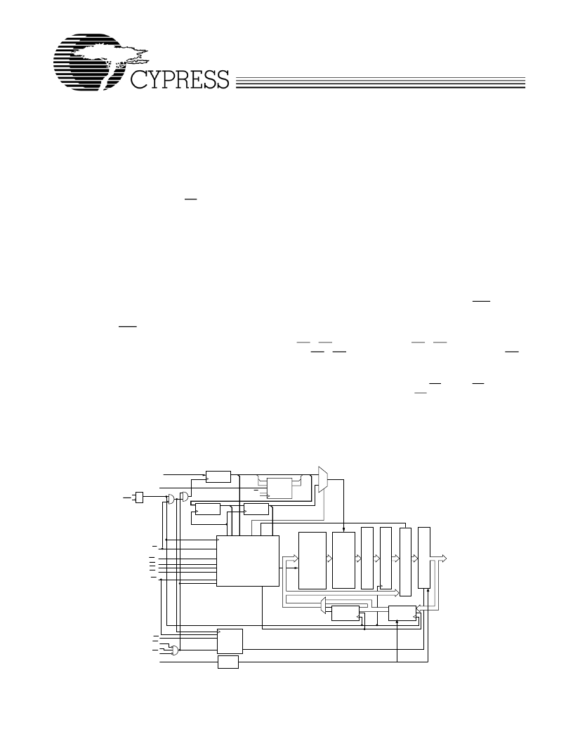
Logic Block Diagram-CY7C1470V33 (2M x 36)
A0, A1, A
C
MODE
BW
a
BW
b
BW
c
BW
d
WE
CE1
CE2
CE3
OE
READ LOGIC
DQs
DQP
a
DQP
b
DQP
c
DQP
d
D
A
T
A
S
T
E
E
R
I
N
G
O
U
T
P
U
T
B
U
F
F
E
R
S
ARRAY
E
E
INPUT
REGISTER 0
ADDRESS
REGISTER 0
WRITE ADDRESS
REGISTER 1
WRITE ADDRESS
REGISTER 2
WRITE REGISTRY
AND DATA COHERENCY
CONTROL LOGIC
BURST
LOGIC
A0'
A1'
D1
D0
Q1
Q0
A0
A1
C
ADV/LD
ADV/LD
E
INPUT
REGISTER 1
S
E
N
S
E
A
M
P
S
E
CLK
CEN
WRITE
DRIVERS
ZZ
SLEEP
CONTROL
O
U
T
P
U
T
R
E
G
I
S
T
E
R
S
相關PDF資料 |
PDF描述 |
|---|---|
| CY7C1472V33-250BZC | 72-Mbit (2M x 36/4M x 18/1M x 72) Pipelined SRAM with NoBL Architecture |
| CY7C1472V33-250BZXC | 72-Mbit (2M x 36/4M x 18/1M x 72) Pipelined SRAM with NoBL Architecture |
| CY7C1474V33 | 72-Mbit (2M x 36/4M x 18/1M x 72) Pipelined SRAM with NoBL Architecture |
| CY7C1474V33-167BGC | 72-Mbit (2M x 36/4M x 18/1M x 72) Pipelined SRAM with NoBL Architecture |
| CY7C1474V33-167BGI | 72-Mbit (2M x 36/4M x 18/1M x 72) Pipelined SRAM with NoBL Architecture |
相關代理商/技術參數(shù) |
參數(shù)描述 |
|---|---|
| CY7C1472XC | 制造商:Cypress Semiconductor 功能描述: |
| CY7C147-35KMB | 制造商:Cypress Semiconductor 功能描述: |
| CY7C1473BV33-133AXC | 功能描述:靜態(tài)隨機存取存儲器 72MB (4Mx18) 3.3v 133MHz 靜態(tài)隨機存取存儲器 RoHS:否 制造商:Cypress Semiconductor 存儲容量:16 Mbit 組織:1 M x 16 訪問時間:55 ns 電源電壓-最大:3.6 V 電源電壓-最小:2.2 V 最大工作電流:22 uA 最大工作溫度:+ 85 C 最小工作溫度:- 40 C 安裝風格:SMD/SMT 封裝 / 箱體:TSOP-48 封裝:Tray |
| CY7C1474BV25-167BGC | 功能描述:靜態(tài)隨機存取存儲器 1Mx72, 2.5V NoBL PL RoHS:否 制造商:Cypress Semiconductor 存儲容量:16 Mbit 組織:1 M x 16 訪問時間:55 ns 電源電壓-最大:3.6 V 電源電壓-最小:2.2 V 最大工作電流:22 uA 最大工作溫度:+ 85 C 最小工作溫度:- 40 C 安裝風格:SMD/SMT 封裝 / 箱體:TSOP-48 封裝:Tray |
| CY7C1474BV25-167BGCT | 功能描述:靜態(tài)隨機存取存儲器 1Mx72, 2.5V NoBL PL RoHS:否 制造商:Cypress Semiconductor 存儲容量:16 Mbit 組織:1 M x 16 訪問時間:55 ns 電源電壓-最大:3.6 V 電源電壓-最小:2.2 V 最大工作電流:22 uA 最大工作溫度:+ 85 C 最小工作溫度:- 40 C 安裝風格:SMD/SMT 封裝 / 箱體:TSOP-48 封裝:Tray |
發(fā)布緊急采購,3分鐘左右您將得到回復。