- 您現(xiàn)在的位置:買賣IC網(wǎng) > PDF目錄67344 > 5962-9957701NXD (TEXAS INSTRUMENTS INC) 4-CH 12-BIT PROPRIETARY METHOD ADC, PARALLEL ACCESS, PDSO32 PDF資料下載
參數(shù)資料
| 型號(hào): | 5962-9957701NXD |
| 廠商: | TEXAS INSTRUMENTS INC |
| 元件分類: | ADC |
| 英文描述: | 4-CH 12-BIT PROPRIETARY METHOD ADC, PARALLEL ACCESS, PDSO32 |
| 封裝: | GREEN, PLASTIC, TSSOP-32 |
| 文件頁(yè)數(shù): | 9/43頁(yè) |
| 文件大小: | 426K |
| 代理商: | 5962-9957701NXD |
第1頁(yè)第2頁(yè)第3頁(yè)第4頁(yè)第5頁(yè)第6頁(yè)第7頁(yè)第8頁(yè)當(dāng)前第9頁(yè)第10頁(yè)第11頁(yè)第12頁(yè)第13頁(yè)第14頁(yè)第15頁(yè)第16頁(yè)第17頁(yè)第18頁(yè)第19頁(yè)第20頁(yè)第21頁(yè)第22頁(yè)第23頁(yè)第24頁(yè)第25頁(yè)第26頁(yè)第27頁(yè)第28頁(yè)第29頁(yè)第30頁(yè)第31頁(yè)第32頁(yè)第33頁(yè)第34頁(yè)第35頁(yè)第36頁(yè)第37頁(yè)第38頁(yè)第39頁(yè)第40頁(yè)第41頁(yè)第42頁(yè)第43頁(yè)

THS1206
SLAS217H – MAY 1999 – REVISED JULY 2003#
www.ti.com
17
Table 2 shows the maximum conversion rate in the single conversion mode.
Table 2. Maximum Conversion Rate in Single Conversion Mode(1)
CHANNEL CONFIGURATION
NUMBER OF
CHANNELS
MAXIMUM CONVERSION
RATE PER CHANNEL
1 single-ended channel
1
3 MSPS
2 single-ended channels
2
2 MSPS
3 single-ended channels
3
1.5 MSPS
4 single-ended channels
4
1.2 MSPS
1 differential channel
1
3 MSPS
2 differential channels
2
2 MSPS
1 single-ended and 1 differential channel
2
2 MSPS
2 single-ended and 1 differential channels
3
1.5 MSPS
(1) Maximum conversion rate with respect to the typical internal oscillator speed (i.e.: 6 MSPS * (tc/t2).
SINGLE CONVERSION MODE
In single conversion mode, a single conversion of the selected analog input channels is performed. The single conversion
mode is selected by setting bit 1 of control register 0 to 1.
A single conversion is initiated by pulsing the CONVST input. On the falling edge of CONVST, the sample and hold stages
of the selected analog inputs are placed into hold simultaneously, and the conversion sequence for the selected channels
is started.
The conversion clock in single conversion mode is generated internally using a clock oscillator circuit. The signal DATA_AV
(data available) becomes active when the trigger level is reached and indicates that the converted sample(s) is (are) written
into the FIFO and can be read out. The trigger level in the single conversion mode can be selected according to Table 13.
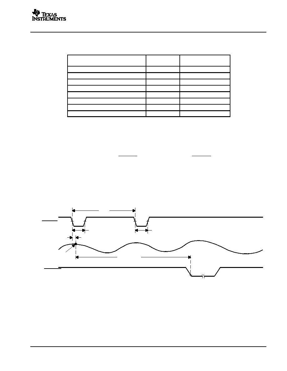
Figure 1 shows the timing of the single conversion mode. In this mode, up to four analog input channels can be selected
to be sampled simultaneously (see Table 2).
CONVST
AIN
Sample N
t1
td(A)
t2
tDATA_AV
DATA_AV,
Trigger Level = 1
Figure 24. Timing of Single Conversion Mode
The time (t2) between consecutive starts of single conversions is dependent on the number of selected analog input
channels. The time tDATA_AV, until DATA_AV becomes active is given by: tDATA_AV = tpipe + n × tc. This equation is valid for
a trigger level which is equivalent to the number of selected analog input channels. For all other trigger level conditions refer
to the timing specifications of single conversion mode.
相關(guān)PDF資料 |
PDF描述 |
|---|---|
| 5962-9958302Q2A | 0.1 A SWITCHING CONTROLLER, 500 kHz SWITCHING FREQ-MAX, CQCC20 |
| 5962-9958301Q2A | 0.1 A SWITCHING CONTROLLER, 500 kHz SWITCHING FREQ-MAX, CQCC20 |
| 5962-9958302QPA | 0.1 A SWITCHING CONTROLLER, 500 kHz SWITCHING FREQ-MAX, CDIP8 |
| TL5001AIP | 0.1 A SWITCHING CONTROLLER, 500 kHz SWITCHING FREQ-MAX, PDIP8 |
| TL5001AIPE4 | 0.1 A SWITCHING CONTROLLER, 500 kHz SWITCHING FREQ-MAX, PDIP8 |
相關(guān)代理商/技術(shù)參數(shù) |
參數(shù)描述 |
|---|---|
| 5962-9958101QXC | 功能描述:LVDS 接口集成電路 RoHS:否 制造商:Texas Instruments 激勵(lì)器數(shù)量:4 接收機(jī)數(shù)量:4 數(shù)據(jù)速率:155.5 Mbps 工作電源電壓:5 V 最大功率耗散:1025 mW 最大工作溫度:+ 85 C 封裝 / 箱體:SOIC-16 Narrow 封裝:Reel |
| 5962-9958301Q2A | 制造商:Texas Instruments 功能描述:DC DC Cntrlr Single-OUT PWM DC to DC Controller 3.6V to 40V Input 20-Pin LCCC Tube |
| 5962-9958301QPA | 制造商:Texas Instruments 功能描述:DC DC Cntrlr Single-OUT PWM DC to DC Controller 3.6V to 40V Input 8-Pin CDIP Tube |
| 5962-9958302Q2A | 制造商:Texas Instruments 功能描述:DC DC Cntrlr Single-OUT PWM DC to DC Controller 3.6V to 40V Input 20-Pin LCCC Tube |
| 5962-9958302QPA | 制造商:Texas Instruments 功能描述:DC DC Cntrlr Single-OUT PWM DC to DC Controller 3.6V to 40V Input 8-Pin CDIP Tube |
發(fā)布緊急采購(gòu),3分鐘左右您將得到回復(fù)。