- 您現(xiàn)在的位置:買賣IC網(wǎng) > PDF目錄67335 > 5962-9318001MRX (MAXIM INTEGRATED PRODUCTS INC) QUAD 1-CHANNEL, SGL POLE DOUBLE THROW SWITCH, CDIP20 PDF資料下載
參數(shù)資料
| 型號(hào): | 5962-9318001MRX |
| 廠商: | MAXIM INTEGRATED PRODUCTS INC |
| 元件分類: | 多路復(fù)用及模擬開關(guān) |
| 英文描述: | QUAD 1-CHANNEL, SGL POLE DOUBLE THROW SWITCH, CDIP20 |
| 封裝: | CERAMIC, DIP-20 |
| 文件頁(yè)數(shù): | 4/19頁(yè) |
| 文件大小: | 3138K |
| 代理商: | 5962-9318001MRX |
第1頁(yè)第2頁(yè)第3頁(yè)當(dāng)前第4頁(yè)第5頁(yè)第6頁(yè)第7頁(yè)第8頁(yè)第9頁(yè)第10頁(yè)第11頁(yè)第12頁(yè)第13頁(yè)第14頁(yè)第15頁(yè)第16頁(yè)第17頁(yè)第18頁(yè)第19頁(yè)

12
Maxim Integrated
Differential Input DirectDrive
Line Drivers/Headphone Amplifiers
MAX97220A–MAX97220E
Detailed Description
The MAX97220_ is a fully differential input line driver/
headphone amplifier for set-top boxes, LCD TV, and
home theater applications where audio fidelity is of pri-
mary importance. Power consumption of the amplifier is
reduced while maintaining high SNR and THD+N per-
formance. The MAX97220A/MAX97220B/MAX97220E
require external input and feedback resistors to set
amplifier gain. The MAX97220C/MAX97220D feature
internal input and feedback resistors for a set gain of
+6dB. Output swings of 3VRMS with a 5V supply and
2VRMS with a 3.3V supply are perfect for line driver
applications.
High fidelity is maintained through the differential input
connection. An output noise voltage of 7FVRMS allows
for 112dB SNR when powered from 5V and 109dB SNR
when powered from 3.3V. The IC has better than 90dB
THD+N across the entire audio bandwidth.
The MAX97220_ operates from a single supply ranging
from 2.5V to 5.5V. An on-chip charge pump inverts the
positive supply (PVDD), creating an equal magnitude
negative supply (PVSS). The headphone amplifiers
operate from bipolar supplies with their outputs biased
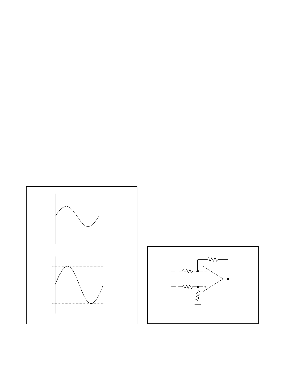
about PGND (Figure 1). The benefit of this PGND bias is
that the amplifier outputs do not have a DC component,
typically PVDD/2. The large DC-blocking capacitors
required with conventional headphone amplifiers are
unnecessary, thus conserving board space, reducing
system cost, and improving frequency response. Output
power of 125mW into 32I is achievable from a 5V sup-
ply. The device features an undervoltage lockout that
prevents operation from an insufficient power supply
and click-and-pop suppression that eliminates audible
transients on startup and shutdown.
Differential Input
The IC can be configured as differential or pseudo-
differential input amplifiers (Figures 2 and 3), making
it compatible with all codecs. A differential input offers
improved noise immunity over a single-ended input. In
devices such as cellular phones, high-frequency signals
from the RF transmitter can couple into the amplifier’s
input traces. The signals appear at the amplifier’s inputs
as common-mode noise. A differential input amplifier
amplifies the difference of the two inputs while signals
common to both inputs are cancelled. Configured dif-
ferentially, the gain of the MAX97220A/MAX97220B/
MAX97220E is set by:
AV = RF/RIN
The common-mode rejection ratio (CMRR) is limited by
the external resistor matching, and if used, input capaci-
tor matching at low frequencies. For example, the worst-
case variation of 1% tolerant resistors results in 40dB
CMRR, while 0.1% resistors result in 60dB CMRR. For
best matching, use resistor arrays.
Figure 1. Conventional Driver Output Waveform vs.
MAX97220_ Output Waveform
Figure 2. Differential Input Configuration
VOUT
PVDD
PVDD/2
PGND
VOUT
+PVDD
-PVDD
DirectDrive BIASING SCHEME
CONVENTIONAL DRIVER-BIASING SCHEME
OUT
RF1*
RIN1*
IN-
IN+
RIN2
RIN1 = RIN2, RF1 = RF2
*RIN1 AND RF1 ARE INTERNAL FOR MAX97220C/MAX97220D
RF2
相關(guān)PDF資料 |
PDF描述 |
|---|---|
| 5962-9204201MXC | 8-CHANNEL, SGL ENDED MULTIPLEXER, DFP16 |
| 5962-9204201MEA | 8-CHANNEL, SGL ENDED MULTIPLEXER, CDIP16 |
| 5962-9204202M2C | DUAL 4-CHANNEL, DIFFERENTIAL MULTIPLEXER, CQCC20 |
| 5962-9204202MXA | DUAL 4-CHANNEL, DIFFERENTIAL MULTIPLEXER, DFP16 |
| 5962-9204202MXC | DUAL 4-CHANNEL, DIFFERENTIAL MULTIPLEXER, DFP16 |
相關(guān)代理商/技術(shù)參數(shù) |
參數(shù)描述 |
|---|---|
| 5962-9318201M2A | 制造商:Texas Instruments 功能描述:OP Amp Quad GP R-R O/P 制造商:Texas Instruments 功能描述:OP AMP QUAD GP R-R O/P 8V/16V 20LCCC - Rail/Tube |
| 5962-9318201QDA | 制造商:Texas Instruments 功能描述: |
| 5962-9318202Q2A | 制造商:Texas Instruments 功能描述:OP Amp Quad GP R-R O/P 制造商:Texas Instruments 功能描述:OP AMP QUAD GP R-R O/P 8V/16V 20LCCC - Rail/Tube |
| 5962-9318202QCA | 制造商:Texas Instruments 功能描述:OP Amp Quad GP R-R O/P 制造商:Rochester Electronics LLC 功能描述:- Bulk |
| 5962-9318301Q2A | 制造商:Texas Instruments 功能描述:Single Transmitter/Receiver RS-485 20-Pin LCCC 制造商:Rochester Electronics LLC 功能描述:- Bulk |
發(fā)布緊急采購(gòu),3分鐘左右您將得到回復(fù)。