- 您現(xiàn)在的位置:買賣IC網(wǎng) > PDF目錄67320 > 5962-0053001HXC DUAL 1-CH 12-BIT PROPRIETARY METHOD ADC, SERIAL ACCESS, CQFP68 PDF資料下載
參數(shù)資料
| 型號: | 5962-0053001HXC |
| 元件分類: | ADC |
| 英文描述: | DUAL 1-CH 12-BIT PROPRIETARY METHOD ADC, SERIAL ACCESS, CQFP68 |
| 封裝: | CERAMIC, LCC-68 |
| 文件頁數(shù): | 2/20頁 |
| 文件大小: | 4809K |
| 代理商: | 5962-0053001HXC |
REV. A
AD13280
–10–
AMP-IN-B-1 when an input of
±0.5 V full scale is desired. Use
AMP-IN-A-2 or AMP-IN-B-2 when
±1 V full scale is desired. Each
channel has an AMP-OUT that must be tied to either a noninver-
ting or inverting input of a differential amplifier with the remaining
input grounded. For example, Side A, AMP-OUT-A (Pin 6) must
be tied to A+IN (Pin 5) with A–IN (Pin 4) tied to ground for
noninverting operation or AMP-OUT-A (Pin 6) tied to A–IN
(Pin 4) with A+IN (Pin 5) tied to ground for inverting operation.
USING THE DIFFERENTIAL INPUT
Each channel of the AD13280 was designed with two optional
differential inputs, A+IN, A–IN and B+IN, B–IN. The inputs
provide system designers with the ability to bypass the AD8037
amplifier and drive the AD8138 directly. The AD8138 differen-
tial ADC driver can be deployed in either a single-ended or
differential input configuration. The differential analog inputs
have a nominal input impedance of 620
and nominal full-
scale input range of 1.2 V p-p. The AD8138 amplifier drives a
differential filter and the custom analog-to-digital converter. The
differential input configuration provides the lowest even-order
harmonics and signal-to-noise (SNR) performance improvement
of up to 3 dB (SNR = 73 dBFS). Exceptional care was taken in
the layout of the differential input signal paths. The differential
input transmission line characteristics are matched and balanced.
Equal attention to system level signal paths must be provided in
order to realize significant performance improvements.
APPLYING THE AD13280
Encoding the AD13280
The AD13280 encode signal must be a high quality, extremely
low phase noise source, to prevent degradation of performance.
Maintaining 12-bit accuracy at 80 MSPS places a premium on
encode clock phase noise. SNR performance can easily degrade
3 dB to 4 dB with 37 MHz input signals when using a high jitter
clock source. See Analog Devices’ Application Note AN-501,
Aperture Uncertainty and ADC System Performance, for complete
details. For optimum performance, the AD13280 must be clocked
differentially. The encode signal is usually ac-coupled into the
ENCODE and
ENCODE pins via a transformer or capacitors.
These pins are biased internally and require no additional bias.
Figure 6 shows one preferred method for clocking the AD13280.
The clock source (low jitter) is converted from single-ended to
differential using an RF transformer. The back-to-back Schottky
diodes across the transformer secondary limit clock excursions
into the AD13280 to approximately 0.8 V p-p differential. This
helps prevent the large voltage swings of the clock from feeding
through to the other portions of the AD13280, and limits the
noise presented to the ENCODE inputs. A crystal clock oscillator
can also be used to drive the RF transformer if an appropriate
limited resistor (typically 100
) is placed in the series with
the primary.
T1-4T
100
0.1 F
ENCODE
AD13280
HSMS2812
DIODES
CLOCK
SOURCE
Figure 6. Crystal Clock Oscillator—Differential Encode
If a low jitter ECL/PECL clock is available, another option is to
ac-couple a differential ECL/PECL signal to the encode input
pins as shown below. A device that offers excellent jitter perfor-
mance is the MC100LVEL16 (or same family) from Motorola.
ENCODE
AD13280
0.1 F
ECL/PECL
VT
0.1 F
Figure 7. Differential ECL for Encode
Jitter Consideration
The signal-to-noise ratio (SNR) for any ADC can be predicted.
When normalized to ADC codes, Equation 1 accurately predicts
the SNR based on three terms. These are jitter, average DNL error,
and thermal noise. Each of these terms contributes to the noise
within the converter.
SNR
f
t
V
N
ANALOG
rms
NOISE rms
N
=×
+
()
+× ×
×
+
–
log
(
)
20
1
2
12
ε
π
J
(1)
fANALOG
= analog input frequency
tJ rms
= rms jitter of the encode (rms sum of encode source
and internal encode circuitry)
ε
= average DNL of the ADC (typically 0.50 LSB)
N
=number of bits in the ADC
VNOISE rms
= the analog input of the ADC (typically 5 LSB)
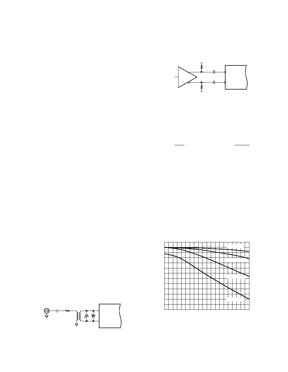
For a 12-bit analog-to-digital converter like the AD13280, aperture
jitter can greatly affect the SNR performance as the analog fre-
quency is increased. The chart below shows a family of curves that
demonstrates the expected SNR performance of the AD13280
as jitter increases. The chart is derived from Equation 1.
For a complete discussion of aperture jitter, please consult Analog
Devices’ Application Note AN-501, Aperture Uncertainty and
ADC System Performance.
CLOCK JITTER – ps
0.0
0.2
0.6
1.0
1.4
1.8
2.2
2.6
3.0
3.4
0.4
0.8
1.2
1.6
2.0
2.4
2.8
3.2
3.6
SNR
–
–dBFS
60
AIN = 5MHz
AIN = 10MHz
AIN = 20MHz
AIN = 37MHz
61
62
63
64
65
66
67
68
69
70
71
59
58
3.8
4.0
Figure 8. SNR vs. Jitter
相關(guān)PDF資料 |
PDF描述 |
|---|---|
| 5962-005300HXA | DUAL 1-CH 12-BIT PROPRIETARY METHOD ADC, PARALLEL ACCESS, CQFP68 |
| 5962-005300HXX | DUAL 1-CH 12-BIT PROPRIETARY METHOD ADC, PARALLEL ACCESS, CQFP68 |
| 5962-0150601HXX | DUAL 1-CH 14-BIT PROPRIETARY METHOD ADC, PARALLEL ACCESS, CQFP68 |
| 5962-0251002HXC | 1-OUTPUT 8 W DC-DC REG PWR SUPPLY MODULE |
| 5962-9213902HZC | 1-OUTPUT 12 W DC-DC REG PWR SUPPLY MODULE |
相關(guān)代理商/技術(shù)參數(shù) |
參數(shù)描述 |
|---|---|
| 5962005304899 | 制造商: 功能描述: 制造商:undefined 功能描述: |
| 5962005308115 | 制造商: 功能描述: 制造商:undefined 功能描述: |
| 5962005345643 | 制造商: 功能描述: 制造商:undefined 功能描述: |
| 5962-0053901QYA | 制造商:TI 制造商全稱:Texas Instruments 功能描述:DIGITAL SIGNAL PROCESSOR |
| 5962-0053901QYC | 制造商:TI 制造商全稱:Texas Instruments 功能描述:DIGITAL SIGNAL PROCESSOR |
發(fā)布緊急采購,3分鐘左右您將得到回復(fù)。