- 您現(xiàn)在的位置:買賣IC網(wǎng) > PDF目錄371399 > 24LCS21 (Microchip Technology Inc.) 1K 2.5V Dual Mode I 2 C Serial EEPROM PDF資料下載
參數(shù)資料
| 型號: | 24LCS21 |
| 廠商: | Microchip Technology Inc. |
| 英文描述: | 1K 2.5V Dual Mode I 2 C Serial EEPROM |
| 中文描述: | 一千2.5V的雙模式的I 2 C串行EEPROM |
| 文件頁數(shù): | 4/12頁 |
| 文件大小: | 91K |
| 代理商: | 24LCS21 |

24LCS21
DS21127B-page 4
1996 Microchip Technology Inc.
2.0
FUNCTIONAL DESCRIPTION
The
Transmit-Only Mode and the bi-directional Mode. There
is a separate two wire protocol to support each mode,
each having a separate clock input but sharing a com-
mon data line (SDA). The device enters the Trans-
mit-Only Mode upon power-up. In this mode, the device
transmits data bits on the SDA pin in response to a
clock signal on the VCLK pin. The device will remain in
this mode until a valid high to low transition is placed on
the SCL input. When a valid transition on SCL is recog-
nized, the device will switch into the bi-directional
Mode. The only way to switch the device back to the
Transmit-Only Mode is to remove power from the
device.
24LCS21
operates
in
two
modes,
the
2.1
Transmit-Only Mode
The device will power up in the Transmit-Only Mode at
address 00H. This mode supports a unidirectional two
wire protocol for continuous transmission of the
contents of the memory array. This device requires that
it be initialized prior to valid data being sent in the Trans-
mit-Only Mode (see Initialization Procedure, below). In
this mode, data is transmitted on the SDA pin in 8-bit
bytes, with each byte followed by a ninth, null bit
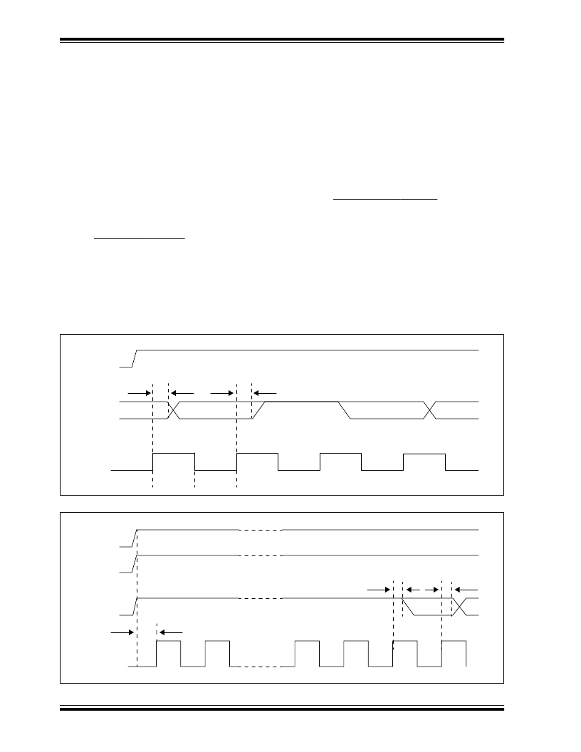
(Figure 2-1). The clock source for the Transmit-Only
Mode is provided on the VCLK pin, and a data bit is out-
put on the rising edge on this pin. The eight bits in each
byte are transmitted most significant bit first. Each byte
within the memory array will be output in sequence.
When the last byte in the memory array is transmitted,
the internal address pointers will wrap around to the
first memory location (00H) and continue. The bi-direc-
tional Mode Clock (SCL) pin must be held high for the
device to remain in the Transmit-Only Mode.
2.2
Initialization Procedure
After V
CC
has stabilized, the device will be in the
Transmit-Only Mode. Nine clock cycles on the VCLK pin
must be given to the device for it to perform internal
sychronization. During this period, the SDA pin will be
in a high impedance state. On the rising edge of the
tenth clock cycle, the device will output the first valid
data bit which will be the most significant bit in address
00h. (Figure 2-2).
FIGURE 2-1: TRANSMIT ONLY MODE
FIGURE 2-2: DEVICE INITIALIZATION
SCL
SDA
VCLK
T
VAA
T
VAA
Bit 1 (LSB)
Null Bit
Bit 1 (MSB)
Bit 7
T
VLOW
T
VHIGH
T
VAA
T
VAA
Bit 8
Bit 7
High Impedance for 9 clock cycles
T
VPU
1
2
8
9
10
11
SCL
SDA
VCLK
Vcc
相關(guān)PDF資料 |
PDF描述 |
|---|---|
| 24LCS41A | 1K/4K 2.5V Dual Mode, Dual Port IIC Serial EEPROM(1K/4K位,2.5V雙模式,雙端口IIC串行EEPROM) |
| 24LCS41 | 1K/4K 2.5V Dual Mode, Dual Port IIC Serial EEPROM(1K/4K位,2.5V雙模式,雙端口IIC串行EEPROM) |
| 24LCS52 | Connectors |
| 24LC52-IP | 2K 2.5V I 2 C Serial EEPROM with Software Write Protect |
| 24LC52-ISN | 2K 2.5V I 2 C Serial EEPROM with Software Write Protect |
相關(guān)代理商/技術(shù)參數(shù) |
參數(shù)描述 |
|---|---|
| 24LCS21A/P | 功能描述:電可擦除可編程只讀存儲器 2.5V Dual Mode RoHS:否 制造商:Atmel 存儲容量:2 Kbit 組織:256 B x 8 數(shù)據(jù)保留:100 yr 最大時鐘頻率:1000 KHz 最大工作電流:6 uA 工作電源電壓:1.7 V to 5.5 V 最大工作溫度:+ 85 C 安裝風格:SMD/SMT 封裝 / 箱體:SOIC-8 |
| 24LCS21A/S | 制造商:Microchip Technology Inc 功能描述:1K 2.5V DUAL MODE SERIAL EEPRO - Gel-pak, waffle pack, wafer, diced wafer on film |
| 24LCS21A/SN | 功能描述:電可擦除可編程只讀存儲器 2.5V Dual Mode RoHS:否 制造商:Atmel 存儲容量:2 Kbit 組織:256 B x 8 數(shù)據(jù)保留:100 yr 最大時鐘頻率:1000 KHz 最大工作電流:6 uA 工作電源電壓:1.7 V to 5.5 V 最大工作溫度:+ 85 C 安裝風格:SMD/SMT 封裝 / 箱體:SOIC-8 |
| 24LCS21A/W | 制造商:Microchip Technology Inc 功能描述:1K 2.5V DUAL MODE SERIAL EEPROM WAFER - Gel-pak, waffle pack, wafer, diced wafer on film |
| 24LCS21A/WF | 制造商:Microchip Technology Inc 功能描述:1K 2.5V DUAL MODE SERIAL EEPRO - Gel-pak, waffle pack, wafer, diced wafer on film |
發(fā)布緊急采購,3分鐘左右您將得到回復(fù)。