- 您現(xiàn)在的位置:買賣IC網(wǎng) > PDF目錄371367 > 20N03HL (Motorola, Inc.) HDTMOS E-FET High Density Power FET DPAK for Surface Mount PDF資料下載
參數(shù)資料
| 型號(hào): | 20N03HL |
| 廠商: | Motorola, Inc. |
| 英文描述: | HDTMOS E-FET High Density Power FET DPAK for Surface Mount |
| 中文描述: | HDTMOS電子FET的高密度功率FET DPAK封裝的表面貼裝 |
| 文件頁(yè)數(shù): | 1/12頁(yè) |
| 文件大?。?/td> | 250K |
| 代理商: | 20N03HL |
1
Motorola, Inc. 1995
# "
! !
N–Channel Enhancement–Mode Silicon Gate
This advanced HDTMOS power FET is designed to withstand
high energy in the avalanche and commutation modes. This new
energy efficient design also offers a drain–to–source diode with a
fast recovery time. Designed for low voltage, high speed switching
applications in power supplies, converters and PWM motor
controls, these devices are particularly well suited for bridge circuits
where diode speed and commutating safe operating areas are
critical and offer additional safety margin against unexpected
voltage transients.
Avalanche Energy Specified
Source–to–Drain Diode Recovery Time Comparable to a Dis-
crete Fast Recovery Diode
Diode is Characterized for Use in Bridge Circuits
IDSS and VDS(on) Specified at Elevated Temperature
Surface Mount Package Available in 16 mm, 13–inch/2500
Unit Tape & Reel, Add T4 Suffix to Part Number
MAXIMUM RATINGS
(TC = 25
°
C unless otherwise noted)
Rating
Symbol
Value
Unit
Drain–Source Voltage
VDSS
VDGR
VGS
VGSM
30
Vdc
Drain–Gate Voltage (RGS = 1.0 M
)
Gate–Source Voltage — Continuous
Gate–Source Voltage
— Non–Repetitive (tp
≤
10 ms)
30
Vdc
±
15
±
20
Vdc
Vpk
Drain Current — Continuous
Drain Current
— Continuous @ 100
°
C
Drain Current
— Single Pulse (tp
≤
10
μ
s)
ID
ID
IDM
20
16
60
Adc
Apk
Total Power Dissipation
Derate above 25
°
C
Total Power Dissipation @ TC = 25
°
C, when mounted with the minimum recommended pad size
PD
74
0.6
1.75
Watts
W/
°
C
Operating and Storage Temperature Range
TJ, Tstg
EAS
–55 to 150
°
C
Single Pulse Drain–to–Source Avalanche Energy — Starting TJ = 25
°
C
(VDD = 25 Vdc, VGS = 5.0 Vdc, Peak IL = 20 Apk, L = 1.0 mH, RG = 25
)
200
mJ
Thermal Resistance — Junction to Case
Thermal Resistance
— Junction to Ambient
Thermal Resistance
— Junction to Ambient, when mounted with the minimum recommended pad size
R
θ
JC
R
θ
JA
R
θ
JA
TL
1.67
100
71.4
°
C/W
Maximum Lead Temperature for Soldering Purposes, 1/8
″
from case for 10 seconds
260
°
C
Designer’s Data for “Worst Case” Conditions
— The Designer’s Data Sheet permits the design of most circuits entirely from the information presented. SOA Limit
curves — representing boundaries on device characteristics — are given to facilitate “worst case” design.
Designer’s, E–FET, and HDTMOS are trademarks of Motorola, Inc. TMOS is a registered trademark of Motorola, Inc.
Thermal Clad is a trademark of the Bergquist Company.
Preferred
devices are Motorola recommended choices for future use and best overall value.
REV 1
Order this document
by MTD20N03HDL/D
SEMICONDUCTOR TECHNICAL DATA
TMOS POWER FET
LOGIC LEVEL
20 AMPERES
30 VOLTS
RDS(on) = 0.035 OHM
Motorola Preferred Device
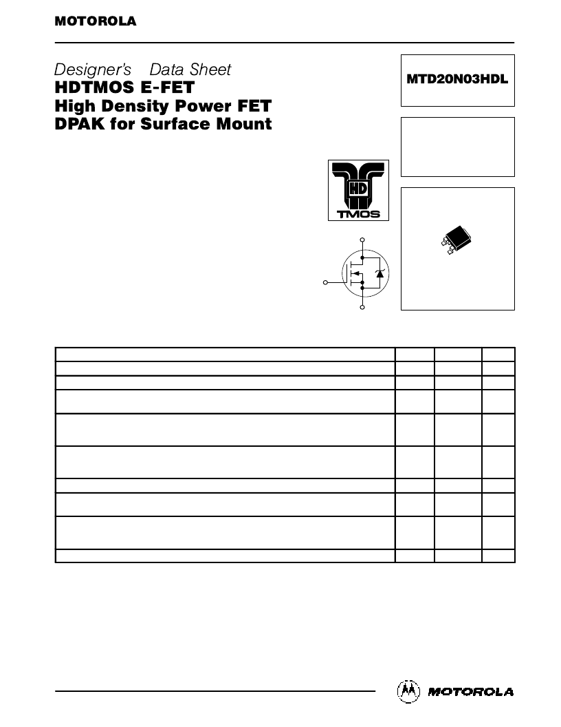
D
S
G
CASE 369A–13, Style 2
DPAK
相關(guān)PDF資料 |
PDF描述 |
|---|---|
| 20N60A4 | 600V, SMPS Series N-Channel IGBTsnull |
| 20NAB06 | 3-phase bridge rectifier +braking chopper +3-phase bridge inverter |
| 20NAB12 | 3-phase bridge rectifier +braking chopper +3-phase bridge inverter |
| 20PMT03 | 10/100 Base TX Transformer Designed for general Chipsets |
| 20PMT04B | Single 10Base-T/100Base-TX Transformer Design for varied turn ratio on Tx side |
相關(guān)代理商/技術(shù)參數(shù) |
參數(shù)描述 |
|---|---|
| 20N0500 | 制造商:Distributed By MCM 功能描述:Pico/Micro .281'' x .093'' |
| 20N06HDT4 | 制造商: 功能描述: 制造商:undefined 功能描述: |
| 20N1000 | 制造商:Distributed By MCM 功能描述:Pico/Micro .281'' x .093'' |
| 20N1500 | 制造商:Distributed By MCM 功能描述:Pico/Micro .281'' x .093'' |
| 20N40 | 制造商:UTC-IC 制造商全稱:UTC-IC 功能描述:400V, 23A N-CHANNEL POWER MOSFET |
發(fā)布緊急采購(gòu),3分鐘左右您將得到回復(fù)。