- 您現(xiàn)在的位置:買賣IC網(wǎng) > PDF目錄225573 > XC7K420T-1LFFG901I (XILINX INC) FPGA, PBGA900 PDF資料下載
參數(shù)資料
| 型號: | XC7K420T-1LFFG901I |
| 廠商: | XILINX INC |
| 元件分類: | FPGA |
| 英文描述: | FPGA, PBGA900 |
| 封裝: | LEAD FREE, FBGA-900 |
| 文件頁數(shù): | 35/50頁 |
| 文件大小: | 1218K |
| 代理商: | XC7K420T-1LFFG901I |
第1頁第2頁第3頁第4頁第5頁第6頁第7頁第8頁第9頁第10頁第11頁第12頁第13頁第14頁第15頁第16頁第17頁第18頁第19頁第20頁第21頁第22頁第23頁第24頁第25頁第26頁第27頁第28頁第29頁第30頁第31頁第32頁第33頁第34頁當前第35頁第36頁第37頁第38頁第39頁第40頁第41頁第42頁第43頁第44頁第45頁第46頁第47頁第48頁第49頁第50頁
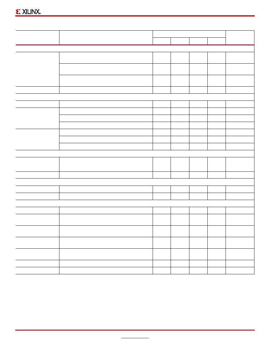
Kintex-7 FPGAs Data Sheet: DC and Switching Characteristics
DS182 (v1.1) April 1, 2011
Advance Product Specification
40
BPI Master Flash Mode Programming Switching
TBPICCO(2)
A[28:00], RS[1:0], FCS_B, FOE_B, FWE_B, ADV_B
outputs valid after CCLK rising edge at 3.3V
ns
A[28:00], RS[1:0], FCS_B, FOE_B, FWE_B, ADV_B
outputs valid after CCLK rising edge at 2.5V
ns
A[28:00], RS[1:0], FCS_B, FOE_B, FWE_B, ADV_B
outputs valid after CCLK rising edge at 1.8V
ns
TBPIDCC/TBPICCD
Setup/Hold on D[15:00] data input pins
5.0/0.0
ns
SPI Master Flash Mode Programming Switching
TSPIDCC/TSPIDCCD
DIN Setup/Hold before/after the rising CCLK edge
5.0/0.0
ns
TSPICCM
MOSI clock to out at 3.3V
ns
MOSI clock to out at 2.5V
ns
MOSI clock to out at 1.8V
ns
TSPICCFC
FCS_B clock to out at 3.3V
ns
FCS_B clock to out at 2.5V
ns
FCS_B clock to out at 1.8V
ns
CCLK Output (Master Modes)
FMCCK_START
Master CCLK frequency at start of configuration
2
MHz, Typ
TMCCKL
Master CCLK clock Low time duty cycle
%, Min/Max
TMCCKH
Master CCLK clock High time duty cycle
%, Min/Max
CCLK Input (Slave Modes)
TSCCKL
Slave CCLK clock minimum Low time
ns, Min
TSCCKH
Slave CCLK clock minimum High time
ns, Min
Dynamic Reconfiguration Port (DRP) for MMCM Before and After DCLK
FDCK
Maximum frequency for DCLK
200
MHz
TMMCMDCK_DADDR/
TMMCMCKD_DADDR
DADDR Setup/Hold
1.25/
0.00
1.40/
0.00
1.63/
0.00
ns
TMMCMDCK_DI/
TMMCMCKD_DI
DI Setup/Hold
1.25/
0.00
1.40/
0.00
1.63/
0.00
ns
TMMCMDCK_DEN/
TMMCMCKD_DEN
DEN Setup/Hold time
1.76/
0.00
1.97/
0.00
2.29/
0.00
ns
TMMCMDCK_DWE/
TMMCMCKD_DWE
DWE Setup/Hold time
1.25/
0.00
1.40/
0.00
1.63/
0.00
ns
TMMCMCKO_DO
CLK to out of DO(3)
3.05
3.54
4.27
ns
TMMCMCKO_DRDY
CLK to out of DRDY
0.37
0.40
0.44
ns
Notes:
1.
To support longer delays in configuration, use the design solutions described in 7 Series FPGA Configuration User Guide.
2.
Only during configuration, the last edge is determined by a weak pull-up/pull-down resistor in the I/O.
3.
DO will hold until next DRP operation.
Table 40: Configuration Switching Characteristics (Cont’d)
Symbol
Description
Speed Grade
Units
-3
-2
-1
-1L
相關(guān)PDF資料 |
PDF描述 |
|---|---|
| XC7K420T-2FFG1156C | FPGA, PBGA1156 |
| XC7K420T-2FFG1156E | FPGA, PBGA1156 |
| XC7K420T-2FFG1156I | FPGA, PBGA1156 |
| XC7K420T-2FFG901C | FPGA, PBGA900 |
| XC7K420T-2FFG901E | FPGA, PBGA900 |
相關(guān)代理商/技術(shù)參數(shù) |
參數(shù)描述 |
|---|---|
| XC7K420T-2FF1156C | 制造商:Xilinx 功能描述:KINTEX-7 - Trays 制造商:Xilinx 功能描述:IC FPGA 400 I/O 1156FCBGA |
| XC7K420T-2FF1156I | 制造商:Xilinx 功能描述:KINTEX-7 - Trays 制造商:Xilinx 功能描述:IC FPGA 400 I/O 1156FCBGA |
| XC7K420T-2FF901C | 制造商:Xilinx 功能描述:KINTEX-7 - Trays 制造商:Xilinx 功能描述:IC FPGA 420K KINTEX-7 901FBGA |
| XC7K420T-2FF901I | 制造商:Xilinx 功能描述:KINTEX-7 - Trays 制造商:Xilinx 功能描述:IC FPGA 380 I/O 901FCBGA |
| XC7K420T-2FFG1156C | 制造商:Xilinx 功能描述:IC FPGA 420K KINTEX-7 1156FBGA |
發(fā)布緊急采購,3分鐘左右您將得到回復(fù)。