- 您現(xiàn)在的位置:買賣IC網(wǎng) > PDF目錄225573 > XC7K420T-1LFFG901C (XILINX INC) FPGA, PBGA900 PDF資料下載
參數(shù)資料
| 型號: | XC7K420T-1LFFG901C |
| 廠商: | XILINX INC |
| 元件分類: | FPGA |
| 英文描述: | FPGA, PBGA900 |
| 封裝: | LEAD FREE, FBGA-900 |
| 文件頁數(shù): | 33/50頁 |
| 文件大?。?/td> | 1218K |
| 代理商: | XC7K420T-1LFFG901C |
第1頁第2頁第3頁第4頁第5頁第6頁第7頁第8頁第9頁第10頁第11頁第12頁第13頁第14頁第15頁第16頁第17頁第18頁第19頁第20頁第21頁第22頁第23頁第24頁第25頁第26頁第27頁第28頁第29頁第30頁第31頁第32頁當(dāng)前第33頁第34頁第35頁第36頁第37頁第38頁第39頁第40頁第41頁第42頁第43頁第44頁第45頁第46頁第47頁第48頁第49頁第50頁
Kintex-7 FPGAs Data Sheet: DC and Switching Characteristics
DS182 (v1.1) April 1, 2011
Advance Product Specification
39
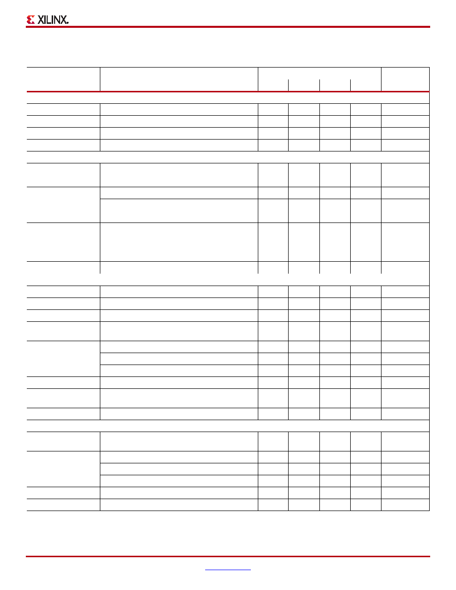
Configuration Switching Characteristics
Table 40: Configuration Switching Characteristics
Symbol
Description
Speed Grade
Units
-3
-2
-1
-1L
Power-up Timing Characteristics
TPL(1)
Program Latency
ms, Max
TPOR(1)
Power-on-Reset
50
ms, Max
TICCK
CCLK (output) delay
ns, Min
TPROGRAM
Program Pulse Width
250
ns, Min
Master/Slave Serial Mode Programming Switching
TDCCK/TCCKD
DIN Setup/Hold, slave mode
5.0/0.0
ns, Min
TDSCCK/TSCCKD
DIN Setup/Hold, master mode
5.0/0.0
ns, Min
TCCO
DOUT at 3.3V
ns, Max
DOUT at 2.5V
ns, Max
DOUT at 1.8V
ns, Max
FMCCK
Maximum Frequency, master mode with respect to
nominal CCLK.
100
MHz,
Max
FMCCKTOL
Frequency Tolerance, master mode with respect to
nominal CCLK.
±55
%
FMSCCK
Slave mode external CCLK
100
MHz
SelectMAP Mode Programming Switching
TSMDCCK/TSMCCKD
SelectMAP Data Setup/Hold
5.0/0.0
ns, Min
TSMCSCCK/TSMCCKCS
CSI_B Setup/Hold
ns, Min
TSMCCKW/TSMWCCK
RDWR_B Setup/Hold
ns, Min
TSMCKCSO
CSO_B clock to out
(330
pull-up resistor required)
ns, Max
TSMCO
CCLK to DATA out in readback at 3.3V
ns, Max
CCLK to DATA out in readback at 2.5V
ns, Max
CCLK to DATA out in readback at 1.8V
ns, Max
FSMCCK
Maximum Frequency with respect to nominal CCLK.
100
MHz, Max
FRBCCK
Maximum Readback Frequency with respect to
nominal CCLK
70
MHz, Max
FMCCKTOL
Frequency Tolerance with respect to nominal CCLK.
±55
%
Boundary-Scan Port Timing Specifications
TTAPTCK/TTCKTAP
TMS and TDI Setup time before TCK/ Hold time after
TCK
ns, Min
TTCKTDO
TCK falling edge to TDO output valid at 3.3V
ns, Max
TCK falling edge to TDO output valid at 2.5V
ns, Max
TCK falling edge to TDO output valid at 1.8V
ns, Max
FTCK
Maximum configuration TCK clock frequency
20
MHz, Max
FTCKB
Maximum boundary-scan TCK clock frequency
20
MHz, Max
相關(guān)PDF資料 |
PDF描述 |
|---|---|
| XC7K420T-1LFFG901E | FPGA, PBGA900 |
| XC7K420T-1LFFG901I | FPGA, PBGA900 |
| XC7K420T-2FFG1156C | FPGA, PBGA1156 |
| XC7K420T-2FFG1156E | FPGA, PBGA1156 |
| XC7K420T-2FFG1156I | FPGA, PBGA1156 |
相關(guān)代理商/技術(shù)參數(shù) |
參數(shù)描述 |
|---|---|
| XC7K420T-2FF1156C | 制造商:Xilinx 功能描述:KINTEX-7 - Trays 制造商:Xilinx 功能描述:IC FPGA 400 I/O 1156FCBGA |
| XC7K420T-2FF1156I | 制造商:Xilinx 功能描述:KINTEX-7 - Trays 制造商:Xilinx 功能描述:IC FPGA 400 I/O 1156FCBGA |
| XC7K420T-2FF901C | 制造商:Xilinx 功能描述:KINTEX-7 - Trays 制造商:Xilinx 功能描述:IC FPGA 420K KINTEX-7 901FBGA |
| XC7K420T-2FF901I | 制造商:Xilinx 功能描述:KINTEX-7 - Trays 制造商:Xilinx 功能描述:IC FPGA 380 I/O 901FCBGA |
| XC7K420T-2FFG1156C | 制造商:Xilinx 功能描述:IC FPGA 420K KINTEX-7 1156FBGA |
發(fā)布緊急采購,3分鐘左右您將得到回復(fù)。