- 您現(xiàn)在的位置:買賣IC網(wǎng) > PDF目錄225573 > XC7K420T-1FFG901E (XILINX INC) FPGA, PBGA900 PDF資料下載
參數(shù)資料
| 型號(hào): | XC7K420T-1FFG901E |
| 廠商: | XILINX INC |
| 元件分類: | FPGA |
| 英文描述: | FPGA, PBGA900 |
| 封裝: | LEAD FREE, FBGA-900 |
| 文件頁數(shù): | 43/50頁 |
| 文件大小: | 1218K |
| 代理商: | XC7K420T-1FFG901E |
第1頁第2頁第3頁第4頁第5頁第6頁第7頁第8頁第9頁第10頁第11頁第12頁第13頁第14頁第15頁第16頁第17頁第18頁第19頁第20頁第21頁第22頁第23頁第24頁第25頁第26頁第27頁第28頁第29頁第30頁第31頁第32頁第33頁第34頁第35頁第36頁第37頁第38頁第39頁第40頁第41頁第42頁當(dāng)前第43頁第44頁第45頁第46頁第47頁第48頁第49頁第50頁
Kintex-7 FPGAs Data Sheet: DC and Switching Characteristics
DS182 (v1.1) April 1, 2011
Advance Product Specification
48
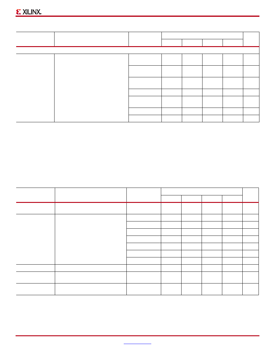
Clock Switching Characteristics
The parameters in this section provide the necessary values for calculating timing budgets for Kintex-7 FPGA clock
transmitter and receiver data-valid windows.
Table 53: Clock-Capable Clock Input Setup and Hold With PLL
Symbol
Description
Device
Speed Grade
Units
-3
-2
-1
-1L
Input Setup and Hold Time Relative to Clock-Capable Clock Input Signal for LVCMOS Standard.(1)
TPSPLLCC/
TPHPLLCC
No Delay clock-capable clock input and
IFF(2) with PLL
XC7K70T
1.75/
–0.50
1.94/
–0.50
2.22/
–0.50
ns
XC7K160T
1.80
–0.49
1.99
–0.49
2.27
–0.49
ns
XC7K325T
1.89
–0.53
2.11
–0.53
2.43
–0.53
ns
XC7K355T
ns
XC7K410T
1.89
–0.53
2.11
–0.53
2.43
–0.53
ns
XC7K420T
ns
XC7K480T
ns
Notes:
1.
Setup and Hold times are measured over worst case conditions (process, voltage, temperature). Setup time is measured relative to the
Global Clock input signal using the slowest process, highest temperature, and lowest voltage. Hold time is measured relative to the Global
Clock input signal using the fastest process, lowest temperature, and highest voltage.
2.
IFF = Input Flip-Flop or Latch
3.
Use IBIS to determine any duty-cycle distortion incurred using various standards.
Table 54: Duty Cycle Distortion and Clock-Tree Skew
Symbol
Description
Device
Speed Grade
Units
-3
-2
-1
-1L
TDCD_CLK
Global Clock Tree Duty Cycle
Distortion(1)
All
0.12
ns
TCKSKEW
Global Clock Tree Skew(2)
XC7K70T
0.18
0.20
0.22
ns
XC7K160T
0.32
0.36
0.40
ns
XC7K325T
0.47
0.52
0.59
ns
XC7K355T
ns
XC7K410T
0.47
0.52
0.59
ns
XC7K420T
ns
XC7K480T
ns
TDCD_BUFIO
I/O clock tree duty cycle distortion
All
0.08
ns
TBUFIOSKEW
I/O clock tree skew across one clock
region
All
0.04
0.03
ns
TDCD_BUFR
Regional clock tree duty cycle
distortion
All
0.15
ns
Notes:
1.
These parameters represent the worst-case duty cycle distortion observable at the pins of the device using LVDS output buffers. For cases
where other I/O standards are used, IBIS can be used to calculate any additional duty cycle distortion that might be caused by asymmetrical
rise/fall times.
2.
The TCKSKEW value represents the worst-case clock-tree skew observable between sequential I/O elements. Significantly less clock-tree
skew exists for I/O registers that are close to each other and fed by the same or adjacent clock-tree branches. Use the Xilinx FPGA_Editor
and Timing Analyzer tools to evaluate clock skew specific to your application.
相關(guān)PDF資料 |
PDF描述 |
|---|---|
| XC7K420T-1FFG901I | FPGA, PBGA900 |
| XC7K420T-1LFFG1156C | FPGA, PBGA1156 |
| XC7K420T-1LFFG1156E | FPGA, PBGA1156 |
| XC7K420T-1LFFG1156I | FPGA, PBGA1156 |
| XC7K420T-1LFFG901C | FPGA, PBGA900 |
相關(guān)代理商/技術(shù)參數(shù) |
參數(shù)描述 |
|---|---|
| XC7K420T-1FFG901I | 制造商:Xilinx 功能描述:KINTEX-7 - Trays 制造商:Xilinx 功能描述:IC FPGA 380 I/O 901FCBGA 制造商:Xilinx 功能描述:IC FPGA 420K KINTEX-7 901FBGA |
| XC7K420T-2FF1156C | 制造商:Xilinx 功能描述:KINTEX-7 - Trays 制造商:Xilinx 功能描述:IC FPGA 400 I/O 1156FCBGA |
| XC7K420T-2FF1156I | 制造商:Xilinx 功能描述:KINTEX-7 - Trays 制造商:Xilinx 功能描述:IC FPGA 400 I/O 1156FCBGA |
| XC7K420T-2FF901C | 制造商:Xilinx 功能描述:KINTEX-7 - Trays 制造商:Xilinx 功能描述:IC FPGA 420K KINTEX-7 901FBGA |
| XC7K420T-2FF901I | 制造商:Xilinx 功能描述:KINTEX-7 - Trays 制造商:Xilinx 功能描述:IC FPGA 380 I/O 901FCBGA |
發(fā)布緊急采購,3分鐘左右您將得到回復(fù)。