參數資料
| 型號: | XC3042L-8VQ100C |
| 廠商: | Xilinx Inc |
| 文件頁數: | 53/76頁 |
| 文件大小: | 0K |
| 描述: | IC FPGA 3.3V C-TEMP 100-VQFP |
| 產品變化通告: | XC3000(L) Discontinuation 01/Feb/2003 |
| 標準包裝: | 450 |
| 系列: | XC3000A/L |
| LAB/CLB數: | 144 |
| RAM 位總計: | 30784 |
| 輸入/輸出數: | 82 |
| 門數: | 3000 |
| 電源電壓: | 3 V ~ 3.6 V |
| 安裝類型: | 表面貼裝 |
| 工作溫度: | 0°C ~ 85°C |
| 封裝/外殼: | 100-TQFP |
| 供應商設備封裝: | 100-VQFP(14x14) |
第1頁第2頁第3頁第4頁第5頁第6頁第7頁第8頁第9頁第10頁第11頁第12頁第13頁第14頁第15頁第16頁第17頁第18頁第19頁第20頁第21頁第22頁第23頁第24頁第25頁第26頁第27頁第28頁第29頁第30頁第31頁第32頁第33頁第34頁第35頁第36頁第37頁第38頁第39頁第40頁第41頁第42頁第43頁第44頁第45頁第46頁第47頁第48頁第49頁第50頁第51頁第52頁當前第53頁第54頁第55頁第56頁第57頁第58頁第59頁第60頁第61頁第62頁第63頁第64頁第65頁第66頁第67頁第68頁第69頁第70頁第71頁第72頁第73頁第74頁第75頁第76頁
R
November 9, 1998 (Version 3.1)
7-59
XC3000 Series Field Programmable Gate Arrays
7
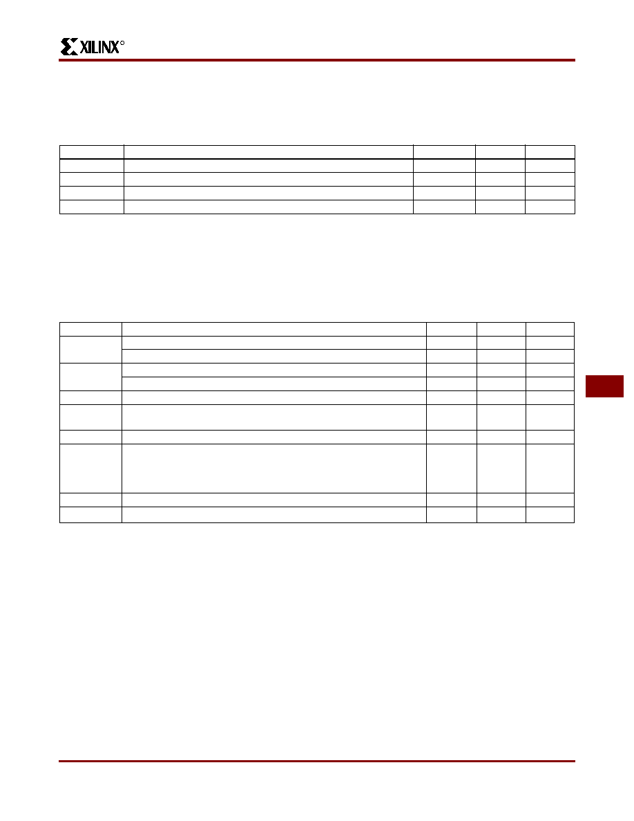
XC3100L Switching Characteristics
Xilinx maintains test specifications for each product as controlled documents. To insure the use of the most recently released
device performance parameters, please request a copy of the current test-specification revision.
XC3100L Operating Conditions
Notes: 1. At junction temperatures above those listed as Operating Conditions, all delay parameters increase by 0.3% per
°C.
2. Although the present (1996) devices operate over the full supply voltage range from 3.0 V to 5.25 V, Xilinx reserves the right
to restrict operation to the 3.0 and 3.6 V range later, when smaller device geometries might preclude operation @ 5 V.
Operating conditions are guaranteed in the 3.0 – 3.6 V VCC range.
XC3100L DC Characteristics Over Operating Conditions
Notes: 1. With no output current loads, no active input or long line pull-up resistors, all package pins at VCC or GND, and the FPGA
configured with a tie option.
2. Total continuous output sink current may not exceed 100 mA per ground pin. Total continuous output source current may not
exceed 100 mA per VCC pin. The number of ground pins varies from the XC3142L to the XC3190L.
3. Not tested. Allows undriven pins to float High. For any other purpose, use an external pull-up.
Symbol
Description
Min
Max
Units
VCC
Supply voltage relative to GND Commercial 0
°C to +85°C junction
3.0
3.6
V
VIH
High-level input voltage
2.0
VCC + 0.3
V
VIL
Low-level input voltage
-0.3
0.8
V
TIN
Input signal transition time
250
ns
Symbol
Description
Min
Max
Units
VOH
High-level output voltage (@ IOH = -4.0 mA, VCC min)
2.4
V
High-level output voltage (@ IOH = -100.0 A, VCC min)
VCC -0.2
V
VOL
Low-level output voltage (@ IOH = 4.0 mA, VCC min)
0.40
V
Low-level output voltage (@ IOH = +100.0 A, VCC min)
0.2
V
VCCPD
Power-down supply voltage (PWRDWN must be Low)
2.30
V
ICCO
Quiescent FPGA supply current
Chip thresholds programmed as CMOS levels1
1.5
mA
IIL
Input Leakage Current
-10
+10
A
CIN
Input capacitance
(sample tested)
All pins except XTL1 and XTL2
XTL1 and XTL2
10
15
pF
IRIN
Pad pull-up (when selected) @ VIN = 0 V
3
0.02
0.17
mA
IRLL
Horizontal long line pull-up (when selected) @ logic Low
0.20
2.80
mA
Product Obsolete or Under Obsolescence
相關PDF資料 |
PDF描述 |
|---|---|
| ABB66DHAN-S621 | CONN EDGECARD 132PS R/A .050 SLD |
| ABB66DHAD-S621 | CONN EDGECARD 132PS R/A .050 SLD |
| ASM43DTAI | CONN EDGECARD 86POS R/A .156 SLD |
| XC3030L-8VQ64I | IC FPGA I-TEMP 3.3V 64-VQFP |
| ASM43DTMI | CONN EDGECARD 86POS R/A .156 SLD |
相關代理商/技術參數 |
參數描述 |
|---|---|
| XC3042L-8VQ100I | 功能描述:IC FPGA 3.3V I-TEMP 100-VQFP RoHS:否 類別:集成電路 (IC) >> 嵌入式 - FPGA(現場可編程門陣列) 系列:XC3000A/L 產品變化通告:XC4000(E,L) Discontinuation 01/April/2002 標準包裝:24 系列:XC4000E/X LAB/CLB數:100 邏輯元件/單元數:238 RAM 位總計:3200 輸入/輸出數:80 門數:3000 電源電壓:4.5 V ~ 5.5 V 安裝類型:表面貼裝 工作溫度:-40°C ~ 100°C 封裝/外殼:120-BCBGA 供應商設備封裝:120-CPGA(34.55x34.55) |
| XC3042PC84BS70C | 制造商:Xilinx 功能描述: |
| XC3042PQ100BKJ9721 | 制造商:XI 功能描述:3042PQ100BK XILINX S9I7B |
| XC3064 | 制造商:XILINX 制造商全稱:XILINX 功能描述:Logic Cell Array Families |
| XC3064100PC84C | 制造商:XILINX 功能描述:NEW |
發(fā)布緊急采購,3分鐘左右您將得到回復。