- 您現(xiàn)在的位置:買賣IC網(wǎng) > PDF目錄4177 > XC3030A-7PC84C (Xilinx Inc)IC LOGIC CL ARRAY 3000GAT 84PLCC PDF資料下載
參數(shù)資料
| 型號(hào): | XC3030A-7PC84C |
| 廠商: | Xilinx Inc |
| 文件頁(yè)數(shù): | 29/76頁(yè) |
| 文件大小: | 0K |
| 描述: | IC LOGIC CL ARRAY 3000GAT 84PLCC |
| 產(chǎn)品變化通告: | Product Discontinuation 27/Apr/2010 |
| 標(biāo)準(zhǔn)包裝: | 1 |
| 系列: | XC3000A/L |
| LAB/CLB數(shù): | 100 |
| RAM 位總計(jì): | 22176 |
| 輸入/輸出數(shù): | 74 |
| 門數(shù): | 2000 |
| 電源電壓: | 4.75 V ~ 5.25 V |
| 安裝類型: | 表面貼裝 |
| 工作溫度: | 0°C ~ 85°C |
| 封裝/外殼: | 84-LCC(J 形引線) |
| 供應(yīng)商設(shè)備封裝: | 84-PLCC |
| 其它名稱: | 122-1018 |
第1頁(yè)第2頁(yè)第3頁(yè)第4頁(yè)第5頁(yè)第6頁(yè)第7頁(yè)第8頁(yè)第9頁(yè)第10頁(yè)第11頁(yè)第12頁(yè)第13頁(yè)第14頁(yè)第15頁(yè)第16頁(yè)第17頁(yè)第18頁(yè)第19頁(yè)第20頁(yè)第21頁(yè)第22頁(yè)第23頁(yè)第24頁(yè)第25頁(yè)第26頁(yè)第27頁(yè)第28頁(yè)當(dāng)前第29頁(yè)第30頁(yè)第31頁(yè)第32頁(yè)第33頁(yè)第34頁(yè)第35頁(yè)第36頁(yè)第37頁(yè)第38頁(yè)第39頁(yè)第40頁(yè)第41頁(yè)第42頁(yè)第43頁(yè)第44頁(yè)第45頁(yè)第46頁(yè)第47頁(yè)第48頁(yè)第49頁(yè)第50頁(yè)第51頁(yè)第52頁(yè)第53頁(yè)第54頁(yè)第55頁(yè)第56頁(yè)第57頁(yè)第58頁(yè)第59頁(yè)第60頁(yè)第61頁(yè)第62頁(yè)第63頁(yè)第64頁(yè)第65頁(yè)第66頁(yè)第67頁(yè)第68頁(yè)第69頁(yè)第70頁(yè)第71頁(yè)第72頁(yè)第73頁(yè)第74頁(yè)第75頁(yè)第76頁(yè)

R
November 9, 1998 (Version 3.1)
7-37
XC3000 Series Field Programmable Gate Arrays
7
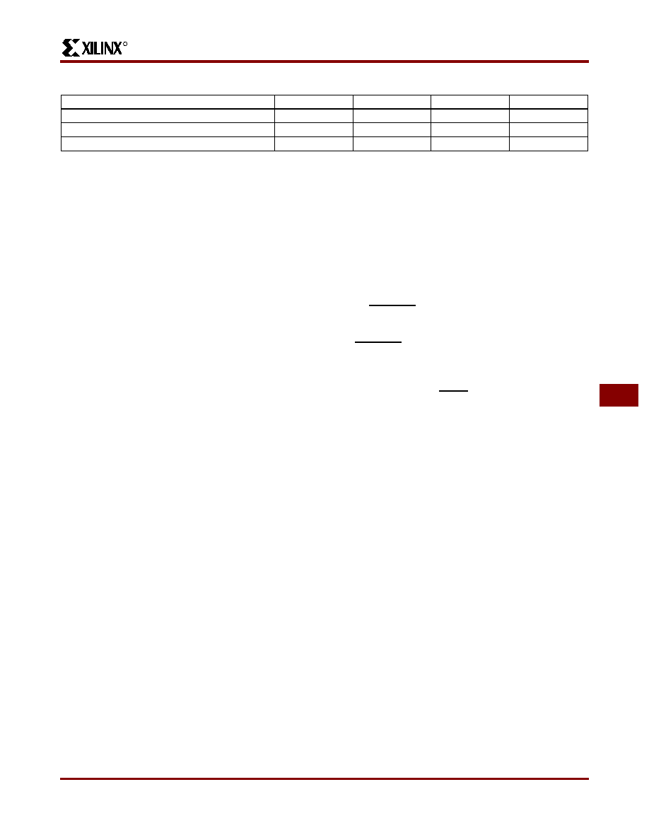
Dynamic Power Consumption
Power Consumption
The Field Programmable Gate Array exhibits the low power
consumption characteristic of CMOS ICs. For any design,
the configuration option of TTL chip input threshold
requires power for the threshold reference. The power
required by the static memory cells that hold the configura-
tion data is very low and may be maintained in a
power-down mode.
Typically, most of power dissipation is produced by external
capacitive loads on the output buffers. This load and fre-
quency dependent power is 25
W/pF/MHz per output.
Another component of I/O power is the external dc loading
on all output pins.
Internal power dissipation is a function of the number and
size of the nodes, and the frequency at which they change.
In an FPGA, the fraction of nodes changing on a given
clock is typically low (10-20%). For example, in a long
binary counter, the total activity of all counter flip-flops is
equivalent to that of only two CLB outputs toggling at the
clock frequency. Typical global clock-buffer power is
between 2.0 mW/MHz for the XC3020A and 3.5 mW/MHz
for the XC3090A. The internal capacitive load is more a
function of interconnect than fan-out. With a typical load of
three general interconnect segments, each CLB output
requires about 0.25 mW per MHz of its output frequency.
Because the control storage of the FPGA is CMOS static
memory, its cells require a very low standby current for data
retention. In some systems, this low data retention current
characteristic can be used as a method of preserving con-
figurations in the event of a primary power loss. The FPGA
has built in powerdown logic which, when activated, will
disable normal operation of the device and retain only the
configuration data. All internal operation is suspended and
output buffers are placed in their high-impedance state with
no pull-ups. Different from the XC3000 family which can be
powered down to a current consumption of a few micro-
amps, the XC3100A draws 5 mA, even in power-down.
This makes power-down operation less meaningful. In con-
trast, ICCPD for the XC3000L is only 10 A.
To force the FPGA into the Powerdown state, the user must
pull the PWRDWN pin Low and continue to supply a reten-
tion voltage to the VCC pins. When normal power is
restored, VCC is elevated to its normal operating voltage
and PWRDWN is returned to a High. The FPGA resumes
operation with the same internal sequence that occurs at
the conclusion of configuration. Internal-I/O and logic-block
storage elements will be reset, the outputs will become
enabled and the DONE/PROG pin will be released.
When VCC is shut down or disconnected, some power
might unintentionally be supplied from an incoming signal
driving an I/O pin. The conventional electrostatic input pro-
tection is implemented with diodes to the supply and
ground. A positive voltage applied to an input (or output)
will cause the positive protection diode to conduct and drive
the VCC connection. This condition can produce invalid
power conditions and should be avoided. A large series
resistor might be used to limit the current or a bipolar buffer
may be used to isolate the input signal.
XC3042A
XC3042L
XC3142A
One CLB driving three local interconnects
0.25
0.17
0.25
mW per MHz
One global clock buffer and clock line
2.25
1.40
1.70
mW per MHz
One device output with a 50 pF load
1.25
mW per MHz
Product Obsolete or Under Obsolescence
相關(guān)PDF資料 |
PDF描述 |
|---|---|
| AGM43DTMS-S189 | CONN EDGECARD 86POS R/A .156 SLD |
| AYM43DTBS-S189 | CONN EDGECARD 86POS R/A .156 SLD |
| ASM43DTBS-S189 | CONN EDGECARD 86POS R/A .156 SLD |
| A14V25A-VQG100C | IC FPGA 2500 GATES 3.3V 100-VQFP |
| A14V25A-VQ100C | IC FPGA 2500 GATES 3.3V 100-VQFP |
相關(guān)代理商/技術(shù)參數(shù) |
參數(shù)描述 |
|---|---|
| XC3030A-7PC84C0100 | 制造商:Xilinx 功能描述: |
| XC3030A-7PC84I | 制造商:XILINX 制造商全稱:XILINX 功能描述:Field Programmable Gate Arrays (XC3000A/L, XC3100A/L) |
| XC3030A-7PQ100C | 功能描述:IC LOGIC CL ARRAY 3000GAT 100PQF RoHS:否 類別:集成電路 (IC) >> 嵌入式 - FPGA(現(xiàn)場(chǎng)可編程門陣列) 系列:XC3000A/L 產(chǎn)品變化通告:XC4000(E,L) Discontinuation 01/April/2002 標(biāo)準(zhǔn)包裝:24 系列:XC4000E/X LAB/CLB數(shù):100 邏輯元件/單元數(shù):238 RAM 位總計(jì):3200 輸入/輸出數(shù):80 門數(shù):3000 電源電壓:4.5 V ~ 5.5 V 安裝類型:表面貼裝 工作溫度:-40°C ~ 100°C 封裝/外殼:120-BCBGA 供應(yīng)商設(shè)備封裝:120-CPGA(34.55x34.55) |
| XC3030A-7PQ100I | 制造商:XILINX 制造商全稱:XILINX 功能描述:Field Programmable Gate Arrays (XC3000A/L, XC3100A/L) |
| XC3030A-7VQ100C | 制造商:Xilinx 功能描述: |
發(fā)布緊急采購(gòu),3分鐘左右您將得到回復(fù)。