- 您現(xiàn)在的位置:買(mǎi)賣(mài)IC網(wǎng) > PDF目錄371302 > X9430WV24I-2.7 (INTERSIL CORP) Dual Digitally Controlled Potentiometer (XDCP) with Operational Amplifier PDF資料下載
參數(shù)資料
| 型號(hào): | X9430WV24I-2.7 |
| 廠商: | INTERSIL CORP |
| 元件分類(lèi): | 數(shù)字電位計(jì) |
| 英文描述: | Dual Digitally Controlled Potentiometer (XDCP) with Operational Amplifier |
| 中文描述: | DUAL 10K DIGITAL POTENTIOMETER, 3-WIRE SERIAL CONTROL INTERFACE, 64 POSITIONS, PDSO24 |
| 封裝: | PLASTIC, TSSOP-24 |
| 文件頁(yè)數(shù): | 7/21頁(yè) |
| 文件大小: | 881K |
| 代理商: | X9430WV24I-2.7 |
第1頁(yè)第2頁(yè)第3頁(yè)第4頁(yè)第5頁(yè)第6頁(yè)當(dāng)前第7頁(yè)第8頁(yè)第9頁(yè)第10頁(yè)第11頁(yè)第12頁(yè)第13頁(yè)第14頁(yè)第15頁(yè)第16頁(yè)第17頁(yè)第18頁(yè)第19頁(yè)第20頁(yè)第21頁(yè)

X9430
– Preliminary Information
Characteristics subject to change without notice.
7 of 21
REV 1.0 6/20/00
www.xicor.com
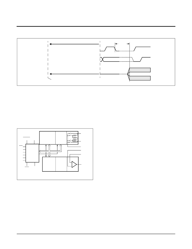
Figure 7. Increment/Decrement Timing
SCK
SI
V
W
INC/DEC CMD Issued
t
WRID
V
OUT
REGISTER OPERATION
Both digitally controlled potentiometers share the serial
interface and share a common architecture. Each
potentiometer is associated with a wiper counter regis-
ter (WCR), and four data registers. Figure 8 illustrates
the control, registers, and system features of the
device.
Figure 8. System Block Diagram
Wiper Counter (WCR) and Analog Control
Registers (ACR)
The X9430 contains two wiper counter registers, one
for each XDCP. The wiper counter register is equivalent
to a serial-in, parallel-out counter with its outputs
decoded to select one of sixty-four switches along its
resistor array. The contents of the wiper counter register
can be altered in four ways: it may be written directly by
the host via the write WCR instruction (serial load); it
may be written indirectly by transferring the contents of
one of four associated data registers (DR) via the XFR
data register instruction (parallel load); it can be modi-
fied one step at a time by the increment/decrement
instruction (WCR only). Finally, it may be loaded with
the contents of its associated data register zero (R0)
upon power-up.
The wiper counter register is a volatile register; that is,
its contents are lost when the X9430 is powered-down.
Although the registers are automatically loaded with
the value in R0 upon power-up, it should be noted this
may be different from the value present at power-down.
Data Registers (DR)
Each potentiometer has four nonvolatile data registers
(DR). These can be read or written directly by the host
and data can be transferred between any of the four
data registers and the WCR. It should be noted all
operations changing data in one of these registers is a
nonvolatile operation and will take a maximum of 10ms.
If the application does not require storage of multiple set-
tings for the potentiometer, these registers can be used
as regular memory locations that could store system
parameters or user preference data.
V
OUT (0,1)
(DR0-DR3)
0,1
Control and
Memory
WCR0
CS
SCK
SO
SI
A1
A0
V
H (0,1)
V
L (0,1)
WP
V
W (0,1)
V
INV (0,1)
V
N (0,1)
+
–
WCR
0,1
V
SS
V
CC
HOLD
WCR1
Detailed Block Diagram
相關(guān)PDF資料 |
PDF描述 |
|---|---|
| X9440WP242.7 | Interface IC |
| X9440WP24I2.7 | Interface IC |
| X9440YP242.7 | Interface IC |
| X9440YP24I2.7 | Interface IC |
| X9440WV24 | Mixed Signal with SPI Interface |
相關(guān)代理商/技術(shù)參數(shù) |
參數(shù)描述 |
|---|---|
| X9430WV24M | 制造商:未知廠家 制造商全稱(chēng):未知廠家 功能描述:Interface IC |
| X9430WV24M2.7 | 制造商:未知廠家 制造商全稱(chēng):未知廠家 功能描述:Interface IC |
| X9438 | 制造商:INTERSIL 制造商全稱(chēng):Intersil Corporation 功能描述:Dual Digitally Controlled Potentiometer (XDCP) with Operational Amplifier |
| X9438WP24 | 制造商:INTERSIL 制造商全稱(chēng):Intersil Corporation 功能描述:Dual Digitally Controlled Potentiometer (XDCP) with Operational Amplifier |
| X9438WP24-2.7 | 制造商:INTERSIL 制造商全稱(chēng):Intersil Corporation 功能描述:Dual Digitally Controlled Potentiometer (XDCP) with Operational Amplifier |
發(fā)布緊急采購(gòu),3分鐘左右您將得到回復(fù)。