- 您現(xiàn)在的位置:買(mǎi)賣(mài)IC網(wǎng) > PDF目錄376443 > X4C105V20I (INTERSIL CORP) RTC Module With CPU Supervisor PDF資料下載
參數(shù)資料
| 型號(hào): | X4C105V20I |
| 廠(chǎng)商: | INTERSIL CORP |
| 元件分類(lèi): | 電源管理 |
| 英文描述: | RTC Module With CPU Supervisor |
| 中文描述: | 1-CHANNEL POWER SUPPLY SUPPORT CKT, PDSO20 |
| 封裝: | PLASTIC, TSSOP-20 |
| 文件頁(yè)數(shù): | 7/19頁(yè) |
| 文件大小: | 296K |
| 代理商: | X4C105V20I |
第1頁(yè)第2頁(yè)第3頁(yè)第4頁(yè)第5頁(yè)第6頁(yè)當(dāng)前第7頁(yè)第8頁(yè)第9頁(yè)第10頁(yè)第11頁(yè)第12頁(yè)第13頁(yè)第14頁(yè)第15頁(yè)第16頁(yè)第17頁(yè)第18頁(yè)第19頁(yè)

7
FN8124.0
March 18, 2005
Acknowledge Polling
The disabling of the inputs during high voltage cycles
can be used to take advantage of the typical 5ms write
cycle time. Once the stop condition is issued to indi-
cate the end of the master’s byte load operation, the
device initiates the internal non volatile write cycle.
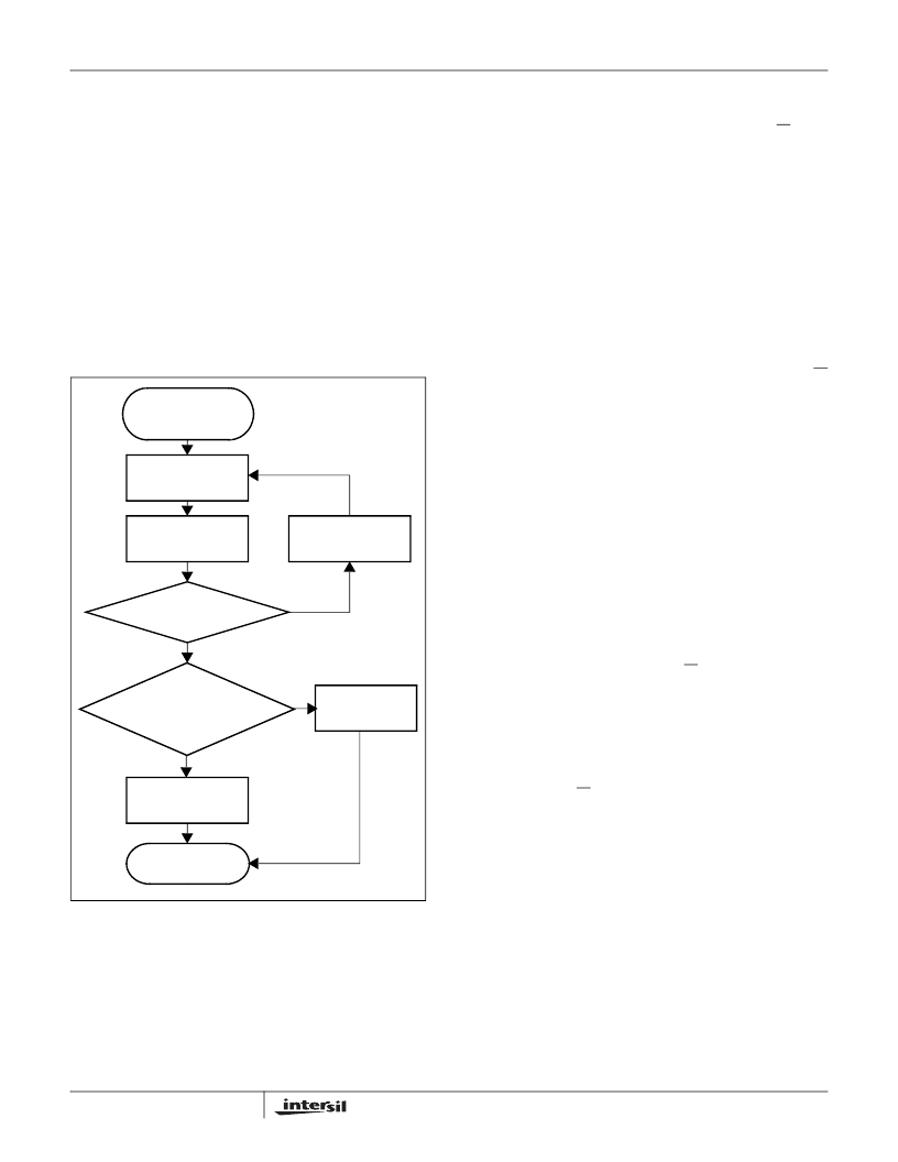
Acknowledge polling can be initiated immediately. To
do this, the master issues a start condition followed by
the slave address byte for a write or read operation. If
the device is still busy with the high voltage cycle then
no ACK will be returned. If the device has completed
the write operation, an ACK will be returned and the
host can then proceed with the read or write operation.
Refer to the flow chart in Figure 8.
Figure 8. Acknowledge Polling Sequence
Serial Read Operations
Read operations are initiated in the same manner as
write operations with the exception that the R/W bit of
the slave address byte is set to one. There are three
basic read operations: current address read, random
read, and sequential read.
Current Address Read
Internally the device contains an address counter that
maintains the address of the last word read incre-
mented by one. Therefore, if the last read was to
address n, the next read operation would access data
from address n+1. On power-up, the address of the
address counter is undefined, requiring a read or write
operation for initialization.
Upon receipt of the slave address byte with the R/W
bit set to one, the device issues an acknowledge and
then transmits the eight bits of the data byte. The mas-
ter terminates the read operation when it does not
respond with an acknowledge during the ninth clock
and then issues a stop condition. Refer to Figure 9 for
the address, acknowledge, and data transfer sequence.
It should be noted that the ninth clock cycle of the read
operation is not a “don’t care.” To terminate a read
operation, the master must either issue a stop condi-
tion during the ninth cycle or hold SDA HIGH during
the ninth clock cycle and then issue a stop condition.
Random Read
A random read operation allows the master to access
any memory location in the array. Prior to issuing the
slave address byte with the R/W bit set to one, the
master must first perform a “dummy” write operation.
The master issues the start condition and the slave
address byte, receives an acknowledge, then issues
the word address byte. After acknowledging receipts
of the word address byte, the master immediately
issues another start condition and the slave address
byte with the R/W bit set to one. This is followed by an
acknowledge from the device and then by the eight bit
word. The master terminates the read operation by not
responding with an acknowledge and then issuing a
stop condition. Refer to Figure 10 for the address,
acknowledge, and data transfer sequence.
ACK
returned
Issue Slave Address
Byte (Read or Write)
Byte load completed
by issuing STOP.
Enter ACK Polling
Issue STOP
Issue START
NO
YES
High Voltage Cycle
complete. Continue
command sequence
Issue STOP
NO
Continue Normal
Read or Write
Command Sequence
PROCEED
YES
X4C105
相關(guān)PDF資料 |
PDF描述 |
|---|---|
| X5329V14Z-4.5A | RTC Module With CPU Supervisor |
| X5648P-4.5A | CAP 270PF 50V CERAMIC MONO 5% |
| X5648 | Thyristor Module |
| X5648P | RTC Module With CPU Supervisor |
| X5648S14 | RTC Module With CPU Supervisor |
相關(guān)代理商/技術(shù)參數(shù) |
參數(shù)描述 |
|---|---|
| X4C105V20I-VTRIP | 制造商:未知廠(chǎng)家 制造商全稱(chēng):未知廠(chǎng)家 功能描述:EEPROM |
| X4C105V20-VTRIP | 制造商:未知廠(chǎng)家 制造商全稱(chēng):未知廠(chǎng)家 功能描述:EEPROM |
| X4C303N1CC | 制造商:SAIA - BURGESS ELECTRONICS INC. 功能描述:Catalogue / X4C303N1CC |
| X4C303N1CCS11 | 制造商:JOHNSON ELECTRIC 功能描述:SWITCH, 3A,125/250VAC, SOLDER 制造商:SAIA - BURGESS ELECTRONICS INC. 功能描述:Catalogue / X4C303N1CCS11 |
| X4C303N8DM | 制造商:SAIA - BURGESS ELECTRONICS INC. 功能描述:Catalogue / X4C303N8DM |
發(fā)布緊急采購(gòu),3分鐘左右您將得到回復(fù)。