- 您現(xiàn)在的位置:買賣IC網(wǎng) > PDF目錄371201 > X24640S8I-2.5 400KHz 2-Wire Serial E 2 PROM with Block Lock PDF資料下載
參數(shù)資料
| 型號(hào): | X24640S8I-2.5 |
| 英文描述: | 400KHz 2-Wire Serial E 2 PROM with Block Lock |
| 中文描述: | 400kHz的2線串行E的2座鎖胎膜早破 |
| 文件頁數(shù): | 6/17頁 |
| 文件大小: | 85K |
| 代理商: | X24640S8I-2.5 |

X24640
6
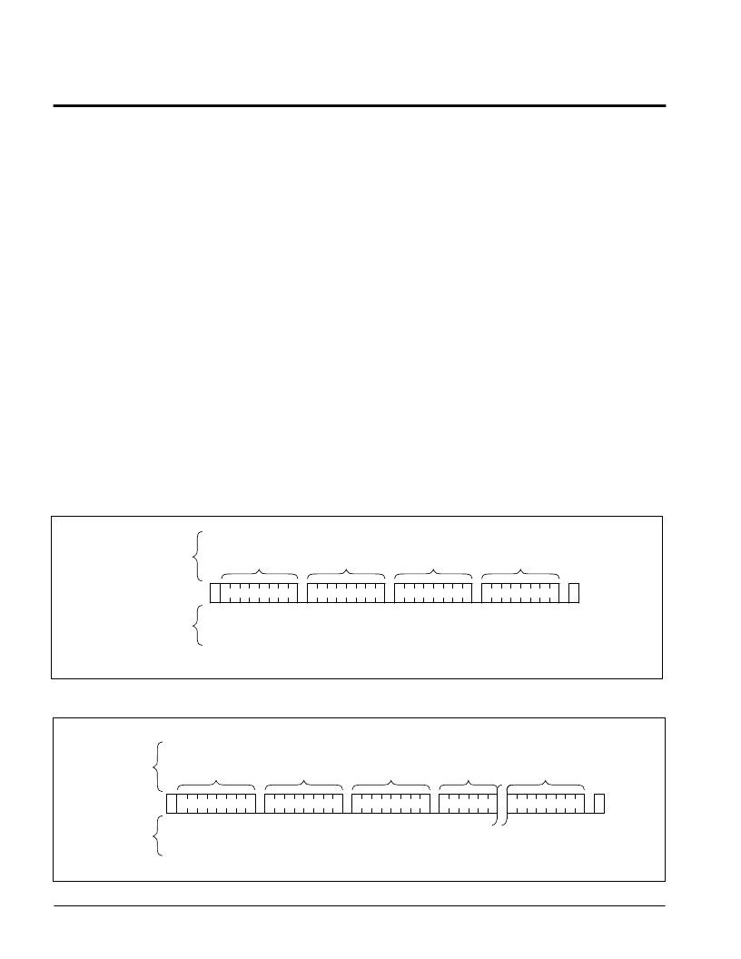
Figure 6. Page Write Sequence
WRITE OPERATIONS
Byte Write
For a write operation, the device requires the Slave
Address Byte, the Word Address Byte 1, and the Word
Address Byte 0, which gives the master access to any
one of the words in the array. Upon receipt of the Word
Address Byte 0, the device responds with an acknowl-
edge, and waits for the first eight bits of data. After
receiving the 8 bits of the data byte, the device again
responds with an acknowledge. The master then
terminates the transfer by generating a stop condition,
at which time the device begins the internal write cycle
to the nonvolatile memory. While the internal write
cycle is in progress the device inputs are disabled
and the device will not respond to any requests from
the master. The SDA pin is at high impedance. See
figure 5.
Page Write
The device is capable of a thirty-two byte page write
operation. It is initiated in the same manner as the byte
write operation; but instead of terminating the write
operation after the first data word is transferred, the
master can transmit up to thirty-one more words. The
device will respond with an acknowledge after the
receipt of each word, and then the byte address is
internally incremented by one. The page address
remains constant. When the counter reaches the end
of the page, it “rolls over” and goes back to the first
byte of the current page. This means that the master
can write 32 words to the page beginning at any byte.
If the master begins writing at byte 16, and loads 32
words, then the first 16 words are written to bytes 16
through 31, and the last 16 words are written to bytes
0 through 15. Afterwards, the address counter would
point to byte 16. If the master writes more than 32
words, then the previously loaded data is overwritten
by the new data, one byte at a time.
The master terminates the data byte loading by
issuing a stop condition, which causes the device to
begin the nonvolatile write cycle. As with the byte write
operation, all inputs are disabled until completion of
the internal write cycle. Refer to figure 6 for the
address, acknowledge, and data transfer sequence.
S
T
A
R
T
SLAVE
ADDRESS
S
T
O
P
P
A
C
K
A
C
K
A
C
K
A
C
K
A
C
K
DATA
(0)
SIGNALS
FROMTHE
MASTER
SDA BUS
SIGNALS
FROMTHE
SLAVE
(n)
WORD ADDRESS
BYTE 1
WORDADDRESS
BYTE 0
0
S
DATA
1 0 1 0
(0
≤
n
≤
31)
7038 FM 08
Figure 5. Byte Write Sequence
SIGNALS
FROMTHE
MASTER
SDA BUS
SIGNALS
FROMTHE
SLAVE
S
T
A
R
T
S
SLAVE
ADDRESS
S
T
O
P
A
C
K
A
C
K
A
C
K
A
C
K
WORDADDRESS
BYTE 1
DATA
1 0 1 0
0
WORD ADDRESS
BYTE 0
P
7038 FM 07
相關(guān)PDF資料 |
PDF描述 |
|---|---|
| X24640P-2.5 | 400KHz 2-Wire Serial E 2 PROM with Block Lock |
| X24641S8I-1.8 | 400 KHz 2-Wire Serial E 2 PROM |
| X24641 | 400 KHz 2-Wire Serial E 2 PROM |
| X24641S8 | 400 KHz 2-Wire Serial E 2 PROM |
| X24641S8-1.8 | 400 KHz 2-Wire Serial E 2 PROM |
相關(guān)代理商/技術(shù)參數(shù) |
參數(shù)描述 |
|---|---|
| X24640V20 | 制造商:XICOR 制造商全稱:Xicor Inc. 功能描述:400KHz 2-Wire Serial E 2 PROM with Block Lock |
| X24640V20-1.8 | 制造商:XICOR 制造商全稱:Xicor Inc. 功能描述:400KHz 2-Wire Serial E 2 PROM with Block Lock |
| X24640V20-2.5 | 制造商:XICOR 制造商全稱:Xicor Inc. 功能描述:400KHz 2-Wire Serial E 2 PROM with Block Lock |
| X24640V20I | 制造商:XICOR 制造商全稱:Xicor Inc. 功能描述:400KHz 2-Wire Serial E 2 PROM with Block Lock |
| X24640V20I-1.8 | 制造商:XICOR 制造商全稱:Xicor Inc. 功能描述:400KHz 2-Wire Serial E 2 PROM with Block Lock |
發(fā)布緊急采購,3分鐘左右您將得到回復(fù)。