- 您現(xiàn)在的位置:買賣IC網(wǎng) > PDF目錄245708 > WS512K32-17NH1MA 512K X 32 MULTI DEVICE SRAM MODULE, 17 ns, HMA66 PDF資料下載
參數(shù)資料
| 型號: | WS512K32-17NH1MA |
| 元件分類: | SRAM |
| 英文描述: | 512K X 32 MULTI DEVICE SRAM MODULE, 17 ns, HMA66 |
| 封裝: | CERAMIC, HIP-66 |
| 文件頁數(shù): | 5/10頁 |
| 文件大小: | 142K |
| 代理商: | WS512K32-17NH1MA |
4
White Electronic Designs Corporation (602) 437-1520 www.whiteedc.com
WS512K32-XXX
AC CHARACTERISTICS
(VCC = 5.0V, VSS = 0V, TA = -55
°C to +125°C)
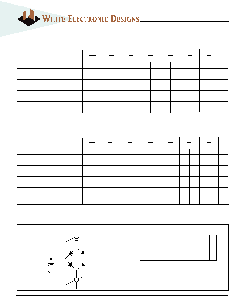
FIG. 4
AC TEST CIRCUIT
NOTES:
VZ is programmable from -2V to +7V.
IOL & IOH programmable from 0 to 16mA.
Tester Impedance Z0 = 75
.
VZ is typically the midpoint of VOH and VOL.
IOL & IOH are adjusted to simulate a typical resistive load circuit.
ATE tester includes jig capacitance.
I
Current Source
D.U.T.
C
= 50 pf
eff
I
OL
V
≈ 1.5V
(Bipolar Supply)
Z
Current Source
OH
AC CHARACTERISTICS
(VCC = 5.0V, VSS = 0V, TA = -55
°C to +125°C)
AC TEST CONDITIONS
Parameter
Typ
Unit
Input Pulse Levels
VIL = 0, VIH = 3.0
V
Input Rise and Fall
5
ns
Input and Output Reference Level
1.5
V
Output Timing Reference Level
1.5
V
Parameter
Symbol
-15*
-17
-20
-25
-35
-45
-55
Units
Write Cycle
Min
Max
Min
Max
Min
Max
Min
Max
Min
Max
Min
Max
Min Max
Write Cycle Time
tWC
15
17
20
25
35
45
55
ns
Chip Select to End of Write
tCW
13
15
17
25
35
50
ns
Address Valid to End of Write
tAW
13
15
17
25
35
50
ns
Data Valid to End of Write
tDW
10
11
12
13
20
25
ns
Write Pulse Width
tWP
13
15
17
25
35
40
ns
Address Setup Time
tAS
2
222
2
ns
Address Hold Time
tAH
0
000
0
5
ns
Output Active from End of Write
tOW1
2
234
4
5
ns
Write Enable to Output in High Z
tWHZ1
8
9
11
13
15
20
ns
Data Hold Time
tDH
0
000
0
ns
* 15ns Access Time available only in Commercial and Industrial Temperature. This speed is not fully characterized and is subject to change without notice.
1. This parameter is guaranteed by design but not tested.
2. The Address Setup Time of minimum 2ns is for the G2T, G1U and H1 packages. tAS minimum for the G4T package is 0ns.
Parameter
Symbol
-15*
-17
-20
-25
-35
-45
-55
Units
Read Cycle
Min
Max
Min
Max
Min
Max
Min
Max
Min
Max
Min
Max
Min
Max
Read Cycle Time
tRC
15
17
20
25
35
45
55
ns
Address Access Time
tAA
15
17
20
25
35
45
55
ns
Output Hold from Address Change
tOH
0
0000
0
ns
Chip Select Access Time
tACS
15
17
20
25
35
45
55
ns
Output Enable to Output Valid
tOE
8
9
10
12
25
ns
Chip Select to Output in Low Z
tCLZ1
2
2244
4
ns
Output Enable to Output in Low Z
tOLZ1
0
0000
0
ns
Chip Disable to Output in High Z
tCHZ1
12
15
20
ns
Output Disable to Output in High Z
tOHZ1
12
15
20
ns
* 15ns Access Time available only in Commercial and Industrial Temperature. This speed is not fully characterized and is subject to change without notice.
1. This parameter is guaranteed by design but not tested.
相關PDF資料 |
PDF描述 |
|---|---|
| WF512K32-90G4TI5A | 512K X 32 FLASH 5V PROM MODULE, 90 ns, CQFP68 |
| WS57C128FB-55CMB | 16K X 8 UVPROM, 55 ns, CQCC32 |
| W24258C-70LL | 32K X 8 STANDARD SRAM, 70 ns, PDIP28 |
| WF2M32-150G2UM5 | 2M X 32 FLASH 5V PROM MODULE, 150 ns, CQFP68 |
| WS1M32V-17G3I | 1M X 32 MULTI DEVICE SRAM MODULE, 17 ns, CQFP84 |
相關代理商/技術參數(shù) |
參數(shù)描述 |
|---|---|
| WS512K32-20G2I | 制造商:未知廠家 制造商全稱:未知廠家 功能描述:x32 SRAM Module |
| WS512K32-20G2M | 制造商:未知廠家 制造商全稱:未知廠家 功能描述:x32 SRAM Module |
| WS512K32-20G2Q | 制造商:未知廠家 制造商全稱:未知廠家 功能描述:x32 SRAM Module |
| WS512K32-20G2TC | 制造商:未知廠家 制造商全稱:未知廠家 功能描述:x32 SRAM Module |
| WS512K32-20G2TCA | 制造商:未知廠家 制造商全稱:未知廠家 功能描述:SRAM|512KX32|CMOS|QFP|68PIN|CERAMIC |
發(fā)布緊急采購,3分鐘左右您將得到回復。