- 您現(xiàn)在的位置:買賣IC網(wǎng) > PDF目錄361880 > WM8199 (Wolfson Microelectronics) 20MSPS 16-bit CCD Digitiser PDF資料下載
參數(shù)資料
| 型號: | WM8199 |
| 廠商: | Wolfson Microelectronics |
| 英文描述: | 20MSPS 16-bit CCD Digitiser |
| 中文描述: | 20MSPS 16位數(shù)字化儀防治荒漠化公約 |
| 文件頁數(shù): | 15/30頁 |
| 文件大?。?/td> | 358K |
| 代理商: | WM8199 |
第1頁第2頁第3頁第4頁第5頁第6頁第7頁第8頁第9頁第10頁第11頁第12頁第13頁第14頁當(dāng)前第15頁第16頁第17頁第18頁第19頁第20頁第21頁第22頁第23頁第24頁第25頁第26頁第27頁第28頁第29頁第30頁
WM8199
OVERALL SIGNAL FLOW SUMMARY
Production Data
w
PD Rev 3.2 November 2003
15
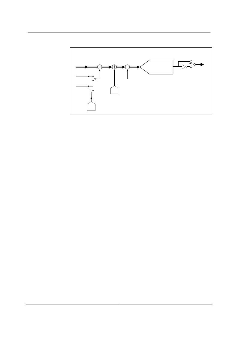
Figure 13 represents the processing of the video signal through the WM8199.
V
RESET
V
VRLC
V
3
CDS = 1
CDS = 0
VRLCEXT=1
260mV*(DAC[7:0]-127.5)/127.5
analog
-
X
++
See parametrics for
DAC voltages.
OP[7:0]
D
1
digital
ADC BLOCK
PGA
BLOCK
OFFSET DAC
BLOCK
V
1
INPUT
SAMPLING
BLOCK
D
2
CDS, VRLCEXT,RLCV[3:0], DAC[7:0],
PGA[7:0], PGAFS[1:0] and INVOP are set
by programming internal control registers.
CDS=1 for CDS, 0 for non-CDS
V
IN
is RINP or GINP or BINP
V
is V
sampled during reset clamp
VRLC is voltage applied to VRLC pin
V
IN
x (65535/V
)
+0 if PGAFS[1:0]=11
+65535 if PGAFS[1:0]=10
+32768 if PGAFS[1:0]=0x
PGA gain
A = 208/(283-PGA[7:0])
OUTPUT
INVERT
BLOCK
D2 = D1 if INVOP = 0
D2 = 65535-D1 if INVOP = 1
Offset
DAC
RLC
DAC
+
V
2
VRLCEXT=0
Figure 13 Overall Signal Flow
The
INPUT
SAMPLING BLOCK
produces an effective input voltage
V
1
. For CDS, this is the
difference between the input video level V
IN
and the input reset level V
RESET
. For non-CDS this is the
difference between the input video level V
IN
and the voltage on the VRLC/VBIAS pin, V
VRLC
,
optionally set via the RLC DAC.
The
OFFSET DAC BLOCK
then adds the amount of fine offset adjustment required to move the
black level of the input signal towards 0V, producing
V
2
.
The
PGA BLOCK
then amplifies the white level of the input signal to maximise the ADC range,
outputting voltage
V
3
.
The
ADC BLOCK
then converts the analogue signal,
V
3
, to a 16-bit unsigned digital output,
D
1
.
The digital output is then inverted, if required, through the
OUTPUT INVERT BLOCK
to produce
D
2.
CALCULATING OUTPUT FOR ANY GIVEN INPUT
The following equations describe the processing of the video and reset level signals through
the WM8199.
INPUT SAMPLING BLOCK: INPUT SAMPLING AND REFERENCING
If CDS = 1, (i.e. CDS operation) the previously sampled reset level, V
RESET
, is subtracted from the
input video.
V
1
=
V
IN
- V
RESET
...................................................................
Eqn. 1
If CDS = 0, (non-CDS operation) the simultaneously sampled voltage on pin VRLC is subtracted
instead.
V
1
=
V
IN
- V
VRLC
.................................................................... Eqn. 2
If VRLCEXT = 1, V
VRLC
is an externally applied voltage on pin VRLC/VBIAS.
If VRLCEXT = 0, V
VRLC
is the output from the internal RLC DAC.
V
VRLC
=
(V
RLCSTEP
RLCV[3:0]) + V
RLCBOT
................................. Eqn. 3
V
RLCSTEP
is the step size of the RLC DAC and V
RLCBOT
is the minimum output of the RLC DAC.
OFFSET DAC BLOCK: OFFSET (BLACK-LEVEL) ADJUST
The resultant signal
V
1
is added to the Offset DAC output.
V
2
=
V
1
+ {260mV
(DAC[7:0]-127.5) } / 127.5 ..................... Eqn. 4
相關(guān)PDF資料 |
PDF描述 |
|---|---|
| WM8199CDR | TVS BIDIRECT 400W 60V SMA |
| WM8199CDS | TVS UNIDIRECT 400W 64V SMA |
| WM8199SCDR | 20MSPS 16-bit CCD Digitiser |
| WM8199SCDS | 20MSPS 16-bit CCD Digitiser |
| WM8716 | High Performance 24-bit, 192kHz Stereo DAC |
相關(guān)代理商/技術(shù)參數(shù) |
參數(shù)描述 |
|---|---|
| WM8199_07 | 制造商:WOLFSON 制造商全稱:WOLFSON 功能描述:20MSPS 16-bit CCD Digitiser |
| WM8199CDR | 制造商:WOLFSON 制造商全稱:WOLFSON 功能描述:20MSPS 16-bit CCD Digitiser |
| WM8199CDS | 制造商:WOLFSON 制造商全稱:WOLFSON 功能描述:20MSPS 16-bit CCD Digitiser |
| WM8199SCDR | 制造商:WOLFSON 制造商全稱:WOLFSON 功能描述:20MSPS 16-bit CCD Digitiser |
| WM8199SCDS | 制造商:WOLFSON 制造商全稱:WOLFSON 功能描述:20MSPS 16-bit CCD Digitiser |
發(fā)布緊急采購,3分鐘左右您將得到回復(fù)。