- 您現(xiàn)在的位置:買賣IC網(wǎng) > PDF目錄361880 > WM8196 (Wolfson Microelectronics) (8+8)BIT OUTPUT 16-BIT CIS/CCD AFE/DIGITISER PDF資料下載
參數(shù)資料
| 型號: | WM8196 |
| 廠商: | Wolfson Microelectronics |
| 英文描述: | (8+8)BIT OUTPUT 16-BIT CIS/CCD AFE/DIGITISER |
| 中文描述: | (8)位輸出16位獨聯(lián)體/防治荒漠化公約AFE的/數(shù)字轉(zhuǎn)換器 |
| 文件頁數(shù): | 17/30頁 |
| 文件大小: | 366K |
| 代理商: | WM8196 |
第1頁第2頁第3頁第4頁第5頁第6頁第7頁第8頁第9頁第10頁第11頁第12頁第13頁第14頁第15頁第16頁當(dāng)前第17頁第18頁第19頁第20頁第21頁第22頁第23頁第24頁第25頁第26頁第27頁第28頁第29頁第30頁
WM8196
Production Data
w
PD Rev 4.1 July 2005
17
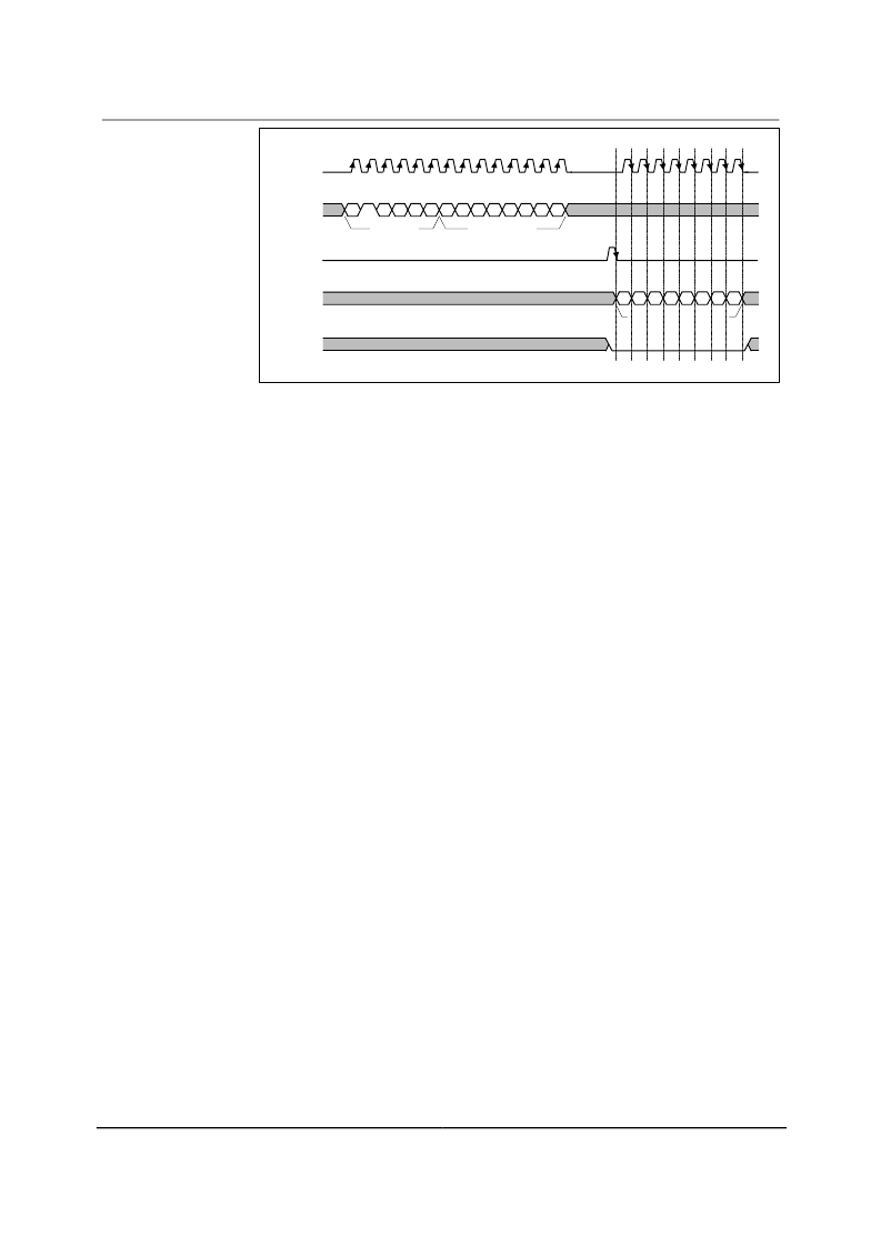
SCK
SEN
SDI
a5
1
a3 a2 a1 a0
Address
x
x
x
Data Word
x
x
x
x
x
d7 d6 d5 d4 d3 d2 d1 d0
Output Data Word
SDO/
OP[7]
OEB
Figure 15 Serial Interface Register Read-back
TIMING REQUIREMENTS
To use this device a master clock (MCLK) of up to 24MHz and a per-pixel synchronisation clock
(VSMP) of up to 12MHz are required. These clocks drive a timing control block, which produces
internal signals to control the sampling of the video signal. MCLK to VSMP ratios and maximum
sample rates for the various modes are shown in Table 4.
PROGRAMMABLE VSMP DETECT CIRCUIT
The VSMP input is used to determine the sampling point and frequency of the WM8196. Under
normal operation a pulse of 1 MCLK period should be applied to VSMP at the desired sampling
frequency (as shown in the Operating Mode Timing Diagrams) and the input sample will be taken on
the first rising MCLK edge after VSMP has gone low. However, in certain applications such a signal
may not be readily available. The programmable VSMP detect circuit in the WM8196 allows the
sampling point to be derived from any signal of the correct frequency, such as a CCD shift register
clock, when applied to the VSMP pin.
When enabled, by setting the VSMPDET control bit, the circuit detects either a rising or falling edge
(determined by POSNNEG control bit) on the VSMP input pin and generates an internal VSMP pulse.
This pulse can optionally be delayed by a number of MCLK periods, specified by the VDEL[2:0] bits.
Figure 16 shows the internal VSMP pulses that can be generated by this circuit for a typical clock
input signal. The internal VSMP pulse is then applied to the timing control block in place of the
normal VSMP pulse provided from the input pin. The sampling point then occurs on the first rising
MCLK edge after this internal VSMP pulse, as shown in the Operating Mode Timing Diagrams.
相關(guān)PDF資料 |
PDF描述 |
|---|---|
| WM8199 | 20MSPS 16-bit CCD Digitiser |
| WM8199CDR | TVS BIDIRECT 400W 60V SMA |
| WM8199CDS | TVS UNIDIRECT 400W 64V SMA |
| WM8199SCDR | 20MSPS 16-bit CCD Digitiser |
| WM8199SCDS | 20MSPS 16-bit CCD Digitiser |
相關(guān)代理商/技術(shù)參數(shù) |
參數(shù)描述 |
|---|---|
| WM8196_07 | 制造商:WOLFSON 制造商全稱:WOLFSON 功能描述:(8 + 8) Bit Output 16-bit CIS/CCD AFE/Digitiser |
| WM8196SCDS | 功能描述:模數(shù)轉(zhuǎn)換器 - ADC 16-Bit 12MSPS 3-Channel AFE RoHS:否 制造商:Texas Instruments 通道數(shù)量:2 結(jié)構(gòu):Sigma-Delta 轉(zhuǎn)換速率:125 SPs to 8 KSPs 分辨率:24 bit 輸入類型:Differential 信噪比:107 dB 接口類型:SPI 工作電源電壓:1.7 V to 3.6 V, 2.7 V to 5.25 V 最大工作溫度:+ 85 C 安裝風(fēng)格:SMD/SMT 封裝 / 箱體:VQFN-32 |
| WM8196SCDS/R | 功能描述:模數(shù)轉(zhuǎn)換器 - ADC 16-Bit 12MSPS 3-Channel AFE RoHS:否 制造商:Texas Instruments 通道數(shù)量:2 結(jié)構(gòu):Sigma-Delta 轉(zhuǎn)換速率:125 SPs to 8 KSPs 分辨率:24 bit 輸入類型:Differential 信噪比:107 dB 接口類型:SPI 工作電源電壓:1.7 V to 3.6 V, 2.7 V to 5.25 V 最大工作溫度:+ 85 C 安裝風(fēng)格:SMD/SMT 封裝 / 箱體:VQFN-32 |
| WM8196SCDS/RV | 功能描述:模數(shù)轉(zhuǎn)換器 - ADC 16-Bit 12MSPS 3-Channel AFE RoHS:否 制造商:Texas Instruments 通道數(shù)量:2 結(jié)構(gòu):Sigma-Delta 轉(zhuǎn)換速率:125 SPs to 8 KSPs 分辨率:24 bit 輸入類型:Differential 信噪比:107 dB 接口類型:SPI 工作電源電壓:1.7 V to 3.6 V, 2.7 V to 5.25 V 最大工作溫度:+ 85 C 安裝風(fēng)格:SMD/SMT 封裝 / 箱體:VQFN-32 |
| WM8196SCDS/V | 功能描述:模數(shù)轉(zhuǎn)換器 - ADC 16-Bit 12MSPS 3-Channel AFE RoHS:否 制造商:Texas Instruments 通道數(shù)量:2 結(jié)構(gòu):Sigma-Delta 轉(zhuǎn)換速率:125 SPs to 8 KSPs 分辨率:24 bit 輸入類型:Differential 信噪比:107 dB 接口類型:SPI 工作電源電壓:1.7 V to 3.6 V, 2.7 V to 5.25 V 最大工作溫度:+ 85 C 安裝風(fēng)格:SMD/SMT 封裝 / 箱體:VQFN-32 |
發(fā)布緊急采購,3分鐘左右您將得到回復(fù)。