- 您現(xiàn)在的位置:買賣IC網(wǎng) > PDF目錄361880 > WM8196 (Wolfson Microelectronics) (8+8)BIT OUTPUT 16-BIT CIS/CCD AFE/DIGITISER PDF資料下載
參數(shù)資料
| 型號: | WM8196 |
| 廠商: | Wolfson Microelectronics |
| 英文描述: | (8+8)BIT OUTPUT 16-BIT CIS/CCD AFE/DIGITISER |
| 中文描述: | (8)位輸出16位獨聯(lián)體/防治荒漠化公約AFE的/數(shù)字轉(zhuǎn)換器 |
| 文件頁數(shù): | 16/30頁 |
| 文件大小: | 366K |
| 代理商: | WM8196 |
第1頁第2頁第3頁第4頁第5頁第6頁第7頁第8頁第9頁第10頁第11頁第12頁第13頁第14頁第15頁當前第16頁第17頁第18頁第19頁第20頁第21頁第22頁第23頁第24頁第25頁第26頁第27頁第28頁第29頁第30頁
WM8196
Production Data
w
PD Rev 4.1 July 2005
16
OUTPUT
FORMAT
8+8-bit
multiplexed
4+4+4+4-bit
(nibble)
MUXOP[1:0]
OUTPUT
PINS
OP[7:0]
OUTPUT
00, 01, 10
A = d15, d14, d13, d12, d11, d10, d9, d8
B = d7, d6, d5, d4, d3, d2, d1,d0
A = d15, d14, d13, d12
B = d11, d10, d9, d8
C = d7, d6, d5, d4
D = d3, d2, d1, d0
11
OP[7:4]
Table 1 Details of Output Data Shown in Figure 12 and Figure 13.
CONTROL INTERFACE
The internal control registers are programmable via the serial digital control interface. The register
contents can be read back via the serial interface on pin OP[7]/SDO.
Note:
It is recommended that a software reset is carried out after the power-up sequence, before
writing to any other register. This ensures that all registers are set to their default values (as shown
in Table 5).
SERIAL INTERFACE: REGISTER WRITE
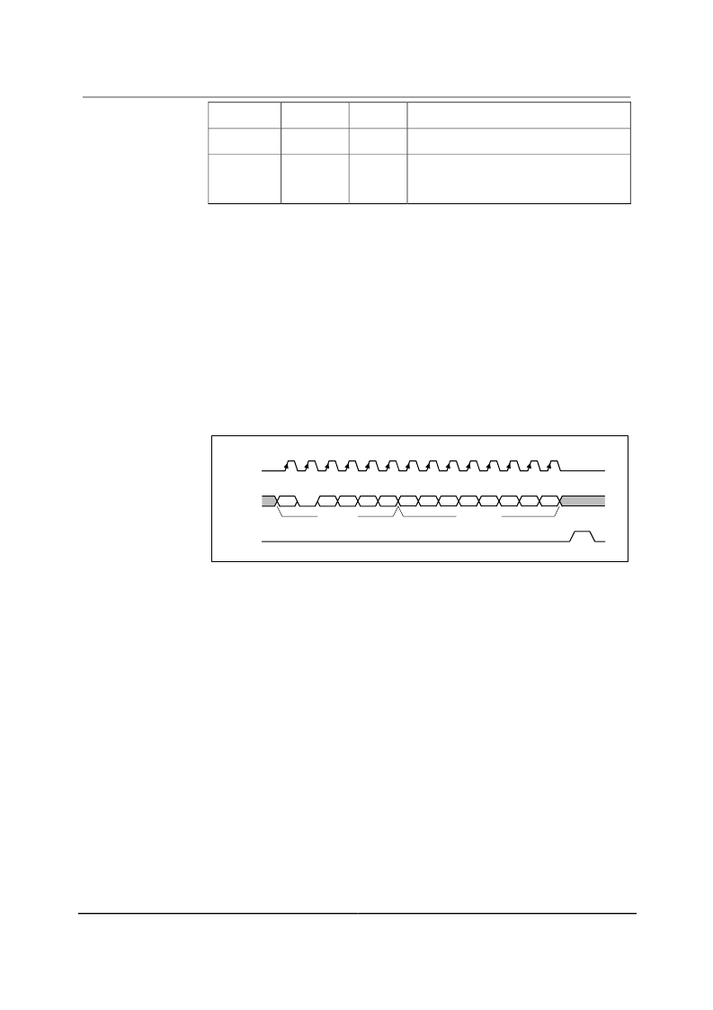
Figure 14 shows register writing in serial mode. Three pins, SCK, SDI and SEN are used. A six-bit
address (a5, 0, a3, a2, a1, a0) is clocked in through SDI, MSB first, followed by an eight-bit data
word (b7, b6, b5, b4, b3, b2, b1, b0), also MSB first. Each bit is latched on the rising edge of SCK.
When the data has been shifted into the device, a pulse is applied to SEN to transfer the data to the
appropriate internal register. Note all valid registers have address bit a4 equal to 0 in write mode.
SCK
SEN
SDI
a5
0
a3
Address
a2
a1
a0
b7
b6
b5
b4
b3
b2
b1
b0
Data Word
Figure 14 Serial Interface Register Write
A software reset is carried out by writing to Address “000100” with any value of data, i.e. Data Word
= XXXXXXXX.
SERIAL INTERFACE: REGISTER READ-BACK
Figure 15 shows register read-back in serial mode. Read-back is initiated by writing to the serial bus
as described above but with address bit a4 set to 1, followed by an 8-bit dummy data word. Writing
address (a5, 1, a3, a2, a1, a0) will cause the contents (d7, d6, d5, d4, d3, d2, d1, d0) of
corresponding register (a5, 0, a3, a2, a1, a0) to be output MSB first on pin SDO (on the falling edge
of SCK). Note that pin SDO is shared with an output pin, OP[7], therefore OEB should always be
held low when register read-back data is expected on this pin. The next word may be read in to SDI
while the previous word is still being output on SDO.
相關(guān)PDF資料 |
PDF描述 |
|---|---|
| WM8199 | 20MSPS 16-bit CCD Digitiser |
| WM8199CDR | TVS BIDIRECT 400W 60V SMA |
| WM8199CDS | TVS UNIDIRECT 400W 64V SMA |
| WM8199SCDR | 20MSPS 16-bit CCD Digitiser |
| WM8199SCDS | 20MSPS 16-bit CCD Digitiser |
相關(guān)代理商/技術(shù)參數(shù) |
參數(shù)描述 |
|---|---|
| WM8196_07 | 制造商:WOLFSON 制造商全稱:WOLFSON 功能描述:(8 + 8) Bit Output 16-bit CIS/CCD AFE/Digitiser |
| WM8196SCDS | 功能描述:模數(shù)轉(zhuǎn)換器 - ADC 16-Bit 12MSPS 3-Channel AFE RoHS:否 制造商:Texas Instruments 通道數(shù)量:2 結(jié)構(gòu):Sigma-Delta 轉(zhuǎn)換速率:125 SPs to 8 KSPs 分辨率:24 bit 輸入類型:Differential 信噪比:107 dB 接口類型:SPI 工作電源電壓:1.7 V to 3.6 V, 2.7 V to 5.25 V 最大工作溫度:+ 85 C 安裝風格:SMD/SMT 封裝 / 箱體:VQFN-32 |
| WM8196SCDS/R | 功能描述:模數(shù)轉(zhuǎn)換器 - ADC 16-Bit 12MSPS 3-Channel AFE RoHS:否 制造商:Texas Instruments 通道數(shù)量:2 結(jié)構(gòu):Sigma-Delta 轉(zhuǎn)換速率:125 SPs to 8 KSPs 分辨率:24 bit 輸入類型:Differential 信噪比:107 dB 接口類型:SPI 工作電源電壓:1.7 V to 3.6 V, 2.7 V to 5.25 V 最大工作溫度:+ 85 C 安裝風格:SMD/SMT 封裝 / 箱體:VQFN-32 |
| WM8196SCDS/RV | 功能描述:模數(shù)轉(zhuǎn)換器 - ADC 16-Bit 12MSPS 3-Channel AFE RoHS:否 制造商:Texas Instruments 通道數(shù)量:2 結(jié)構(gòu):Sigma-Delta 轉(zhuǎn)換速率:125 SPs to 8 KSPs 分辨率:24 bit 輸入類型:Differential 信噪比:107 dB 接口類型:SPI 工作電源電壓:1.7 V to 3.6 V, 2.7 V to 5.25 V 最大工作溫度:+ 85 C 安裝風格:SMD/SMT 封裝 / 箱體:VQFN-32 |
| WM8196SCDS/V | 功能描述:模數(shù)轉(zhuǎn)換器 - ADC 16-Bit 12MSPS 3-Channel AFE RoHS:否 制造商:Texas Instruments 通道數(shù)量:2 結(jié)構(gòu):Sigma-Delta 轉(zhuǎn)換速率:125 SPs to 8 KSPs 分辨率:24 bit 輸入類型:Differential 信噪比:107 dB 接口類型:SPI 工作電源電壓:1.7 V to 3.6 V, 2.7 V to 5.25 V 最大工作溫度:+ 85 C 安裝風格:SMD/SMT 封裝 / 箱體:VQFN-32 |
發(fā)布緊急采購,3分鐘左右您將得到回復。