- 您現(xiàn)在的位置:買賣IC網 > PDF目錄361880 > WM8150CDS (Wolfson Microelectronics) SINGLE CHANNEL 12 BIT CIS/CCD AFE WITH 4 BIT WIDE OUTPUT PDF資料下載
參數(shù)資料
| 型號: | WM8150CDS |
| 廠商: | Wolfson Microelectronics |
| 英文描述: | SINGLE CHANNEL 12 BIT CIS/CCD AFE WITH 4 BIT WIDE OUTPUT |
| 中文描述: | 單通道12位獨聯(lián)體/防治荒漠化公約與4位寬輸出模擬前端 |
| 文件頁數(shù): | 14/24頁 |
| 文件大小: | 271K |
| 代理商: | WM8150CDS |
WM8150
Production Data
w
PD Rev 3.0 November 2002
14
CONTROL INTERFACE
The internal control registers are programmable via the serial digital control interface. The register
contents can be read back via the serial interface on pin OP[3]/SDO.
It is recommended that a software reset is carried out after the power-up sequence, before writing to
any other register. This ensures that all registers are set to their default values (as shown in Table
4).
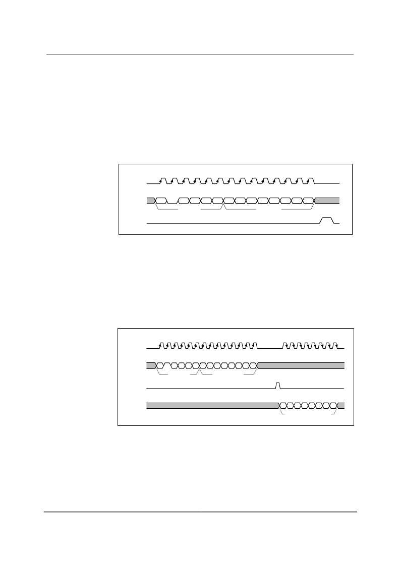
SERIAL INTERFACE: REGISTER WRITE
Figure 12 shows register writing in serial mode. Three pins, SCK, SDI and SEN are used. A six-bit
address (a5, 0, a3, a2, a1, a0) is clocked in through SDI, MSB first, followed by an eight-bit data
word (b7, b6, b5, b4, b3, b2, b1, b0), also MSB first. Each bit is latched on the rising edge of SCK.
When the data has been shifted into the device, a pulse is applied to SEN to transfer the data to the
appropriate internal register. Note all valid registers have address bit a4 equal to 0 in write mode.
SCK
SEN
SDI
a5
0
a3
Address
a2
a1
a0
b7
b6
b5
b4
b3
b2
b1
b0
Data Word
Figure 12 Serial Interface Register Write
A software reset is carried out by writing to Address “000100” with any value of data, (i.e. Data Word
= XXXXXXXX.
SERIAL INTERFACE: REGISTER READ-BACK
Figure 13 shows register read-back in serial mode. Read-back is initiated by writing to the serial bus
as described above but with address bit a4 set to 1, followed by an 8-bit dummy data word. Writing
address (a5, 1, a3, a2, a1, a0) will cause the contents (d7, d6, d5, d4, d3, d2, d1, d0) of
corresponding register (a5, 0, a3, a2, a1, a0) to be output MSB first on pin SDO (on the falling edge
of SCK). Note that pin SDO is shared with an output pin, OP[3], so no data can be read when reading
from a register. The next word may be read in to SDI while the previous word is still being output on
SDO.
SCK
SEN
SDI
a5
1
a3 a2 a1 a0
Address
x
x
x
Data Word
x
x
x
x
x
d7 d6 d5 d4 d3 d2 d1 d0
Output Data Word
SDO
Figure 13 Serial Interface Register Read-back
TIMING REQUIREMENTS
To use this device a master clock (MCLK) of up to 16MHz and a per-pixel synchronisation clock
(VSMP) of up to 8MHz are required. These clocks drive a timing control block, which produces
internal signals to control the sampling of the video signal. MCLK to VSMP ratios and maximum
sample rates for the various modes are shown in Table 3.
相關PDF資料 |
PDF描述 |
|---|---|
| WM8150CDSR | SINGLE CHANNEL 12 BIT CIS/CCD AFE WITH 4 BIT WIDE OUTPUT |
| WM8170 | 5.0 VOLT BI-DIRECTIONAL TRANSIENT VOLTAGE SUPPRESSOR |
| WM8181 | 12-bit 2MSPS Serial Output CIS/CCD Digitiser |
| WM8190 | TVS UNIDIRECT 6V 400W SMA |
| WM8191 | TVS BI-DIR 6.0V 400W SMA |
相關代理商/技術參數(shù) |
參數(shù)描述 |
|---|---|
| WM8150CDS/R | 制造商:WOLFSON 制造商全稱:WOLFSON 功能描述:Single Channel 12-bit CIS/CCD AFE with 4-bit Wide Output |
| WM8150CDSR | 制造商:WOLFSON 制造商全稱:WOLFSON 功能描述:SINGLE CHANNEL 12 BIT CIS/CCD AFE WITH 4 BIT WIDE OUTPUT |
| WM8150SCDS | 功能描述:視頻 IC 12-Bit 6MSPS Single-Channel AFE RoHS:否 制造商:Fairchild Semiconductor 工作電源電壓:5 V 電源電流:80 mA 最大工作溫度:+ 85 C 封裝 / 箱體:TSSOP-28 封裝:Reel |
| WM8150SCDS/R | 功能描述:視頻 IC 12-Bit 6MSPS Single-Channel AFE RoHS:否 制造商:Fairchild Semiconductor 工作電源電壓:5 V 電源電流:80 mA 最大工作溫度:+ 85 C 封裝 / 箱體:TSSOP-28 封裝:Reel |
| WM8150SCDS/RV | 功能描述:模數(shù)轉換器 - ADC 12-Bit 6MSPS Single-Channel AFE RoHS:否 制造商:Texas Instruments 通道數(shù)量:2 結構:Sigma-Delta 轉換速率:125 SPs to 8 KSPs 分辨率:24 bit 輸入類型:Differential 信噪比:107 dB 接口類型:SPI 工作電源電壓:1.7 V to 3.6 V, 2.7 V to 5.25 V 最大工作溫度:+ 85 C 安裝風格:SMD/SMT 封裝 / 箱體:VQFN-32 |
發(fā)布緊急采購,3分鐘左右您將得到回復。