- 您現(xiàn)在的位置:買賣IC網(wǎng) > PDF目錄361880 > WM8150CDS (Wolfson Microelectronics) SINGLE CHANNEL 12 BIT CIS/CCD AFE WITH 4 BIT WIDE OUTPUT PDF資料下載
參數(shù)資料
| 型號: | WM8150CDS |
| 廠商: | Wolfson Microelectronics |
| 英文描述: | SINGLE CHANNEL 12 BIT CIS/CCD AFE WITH 4 BIT WIDE OUTPUT |
| 中文描述: | 單通道12位獨聯(lián)體/防治荒漠化公約與4位寬輸出模擬前端 |
| 文件頁數(shù): | 11/24頁 |
| 文件大?。?/td> | 271K |
| 代理商: | WM8150CDS |
Production Data
WM8150
w
PD Rev 3.0 November 2002
11
ADC INPUT BLACK LEVEL ADJUST
The output from the PGA should be offset to match the full-scale range of the ADC (V
FS
= 2.5V). For
negative-going input video signals, a black level (zero differential) output from the PGA should be
offset to the top of the ADC range by setting register bits PGAFS[1:0]=10. For positive going input
signal the black level should be offset to the bottom of the ADC range by setting PGAFS[1:0]=11.
Bipolar input video is accommodated by setting PGAFS[1:0]=00 or PGAFS[1:0]=01 (zero differential
input voltage gives mid-range ADC output).
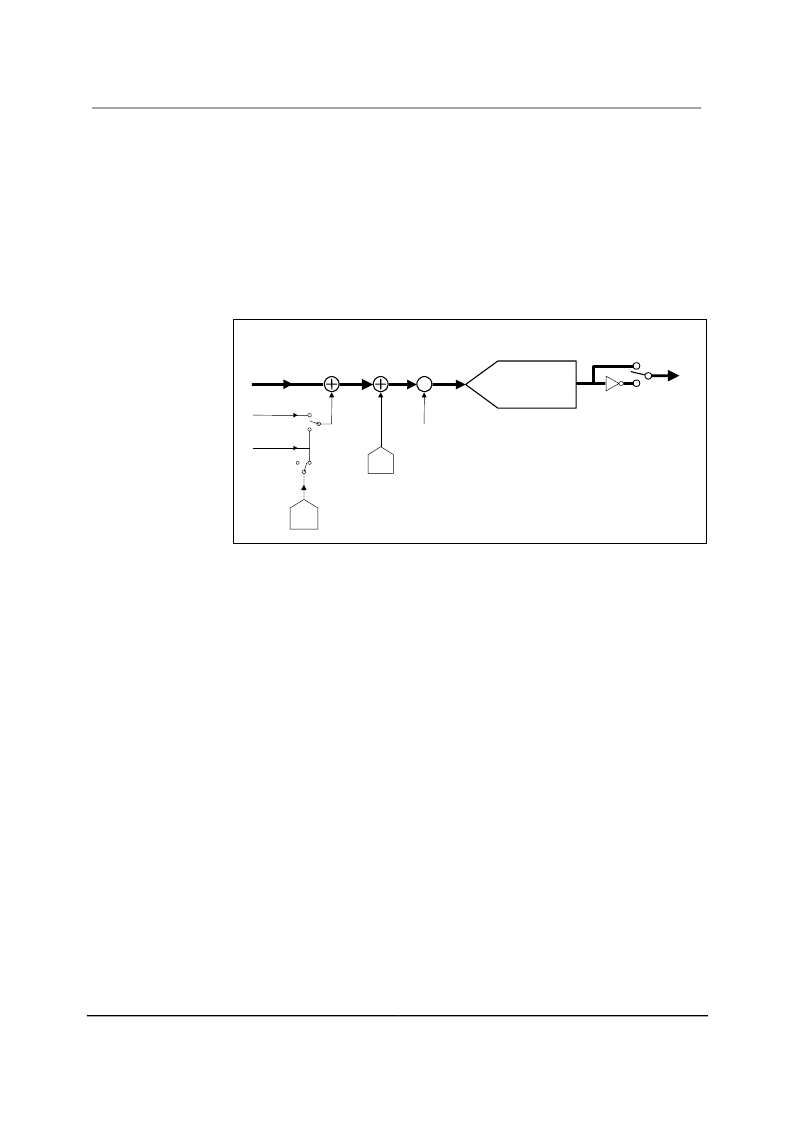
OVERALL SIGNAL FLOW SUMMARY
Figure 9 represents the processing of the video signal through the WM8150.
Figure 9 Overall Signal Flow
The
INPUT SAMPLING BLOCK
produces an effective input voltage
V
1
. For CDS, this is the
difference between the input video level V
IN
and the input reset level V
RESET
. For non-CDS this is the
difference between the input video level V
IN
and the voltage on the VRLC/VBIAS pin, V
VRLC
,
optionally set via the RLC DAC.
The
OFFSET DAC BLOCK
then adds the amount of fine offset adjustment required to move the
black level of the input signal towards 0V, producing
V
2
.
The
PGA BLOCK
then amplifies the white level of the input signal to maximise the ADC range,
outputting voltage
V
3
.
The
ADC BLOCK
then converts the analogue signal,
V
3
, to a 12-bit unsigned digital output,
D
1
.
The digital output is then inverted, if required, through the
OUTPUT INVERT BLOCK
to produce
D
2.
CALCULATING OUTPUT FOR ANY GIVEN INPUT
The following equations describe the processing of the video and reset level signals through
the WM8150.
INPUT SAMPLING BLOCK: INPUT SAMPLING AND REFERENCING
If CDS = 1, (i.e. CDS operation) the previously sampled reset level, V
RESET
, is subtracted from the
input video.
V
1
=
V
IN
- V
RESET
...................................................................
Eqn. 1
If CDS = 0, (non-CDS operation) the simultaneously sampled voltage on pin VRLC is subtracted
instead.
V
1
=
V
IN
- V
VRLC
....................................................................
Eqn. 2
If VRLCEXT = 1, V
VRLC
is an externally applied voltage on pin VRLC/VBIAS.
If VRLCEXT = 0, V
VRLC
is the output from the internal RLC DAC.
V
RESET
V
VRLC
V
3
CDS = 1
CDS = 0
VRLCEXT=1
260mV*(DAC[7:0]-127.5)/127.5
analog
-
X
++
V
RLCSTEP
*RLCV[3:0] + V
RLCBOT
OP[3:0]
D
1
digital
ADC BLOCK
PGA
BLOCK
OFFSET DAC
BLOCK
INPUT
SAMPLING
BLOCK
D
2
CDS, VRLCEXT,RLCV[3:0], DAC[7:0],
PGA[7:0], PGAFS[1:0] and INVOP are set
by programming internal control registers.
CDS=1 for CDS, 0 for non-CDS
V
V
V
IN
is VINP voltage sampled on video sample
RESET
is VINP sampled during reset clamp
VRLC
is voltage applied to VRLC pin
V
IN
x (4095/V
if PGAFS[1:0]=11
+4095 if PGAFS[1:0]=10
+2047 if PGAFS[1:0]=0x
)
+0
PGA gain
A = 0.78+(PGA[7:0]*7.57)/255
OUTPUT
INVERT
BLOCK
D2 = D1 if INVOP = 0
D2 =4095-D1 if INVOP = 1
Offset
DAC
RLC
DAC
+
V
2
V
1
VRLCEXT=0
相關(guān)PDF資料 |
PDF描述 |
|---|---|
| WM8150CDSR | SINGLE CHANNEL 12 BIT CIS/CCD AFE WITH 4 BIT WIDE OUTPUT |
| WM8170 | 5.0 VOLT BI-DIRECTIONAL TRANSIENT VOLTAGE SUPPRESSOR |
| WM8181 | 12-bit 2MSPS Serial Output CIS/CCD Digitiser |
| WM8190 | TVS UNIDIRECT 6V 400W SMA |
| WM8191 | TVS BI-DIR 6.0V 400W SMA |
相關(guān)代理商/技術(shù)參數(shù) |
參數(shù)描述 |
|---|---|
| WM8150CDS/R | 制造商:WOLFSON 制造商全稱:WOLFSON 功能描述:Single Channel 12-bit CIS/CCD AFE with 4-bit Wide Output |
| WM8150CDSR | 制造商:WOLFSON 制造商全稱:WOLFSON 功能描述:SINGLE CHANNEL 12 BIT CIS/CCD AFE WITH 4 BIT WIDE OUTPUT |
| WM8150SCDS | 功能描述:視頻 IC 12-Bit 6MSPS Single-Channel AFE RoHS:否 制造商:Fairchild Semiconductor 工作電源電壓:5 V 電源電流:80 mA 最大工作溫度:+ 85 C 封裝 / 箱體:TSSOP-28 封裝:Reel |
| WM8150SCDS/R | 功能描述:視頻 IC 12-Bit 6MSPS Single-Channel AFE RoHS:否 制造商:Fairchild Semiconductor 工作電源電壓:5 V 電源電流:80 mA 最大工作溫度:+ 85 C 封裝 / 箱體:TSSOP-28 封裝:Reel |
| WM8150SCDS/RV | 功能描述:模數(shù)轉(zhuǎn)換器 - ADC 12-Bit 6MSPS Single-Channel AFE RoHS:否 制造商:Texas Instruments 通道數(shù)量:2 結(jié)構(gòu):Sigma-Delta 轉(zhuǎn)換速率:125 SPs to 8 KSPs 分辨率:24 bit 輸入類型:Differential 信噪比:107 dB 接口類型:SPI 工作電源電壓:1.7 V to 3.6 V, 2.7 V to 5.25 V 最大工作溫度:+ 85 C 安裝風格:SMD/SMT 封裝 / 箱體:VQFN-32 |
發(fā)布緊急采購,3分鐘左右您將得到回復(fù)。