- 您現(xiàn)在的位置:買賣IC網(wǎng) > PDF目錄361880 > WM2618 (Wolfson Microelectronics) Dual 12-Bit Serial Input Voltage Output DAC PDF資料下載
參數(shù)資料
| 型號: | WM2618 |
| 廠商: | Wolfson Microelectronics |
| 英文描述: | Dual 12-Bit Serial Input Voltage Output DAC |
| 中文描述: | 雙12位串行輸入電壓輸出DAC |
| 文件頁數(shù): | 1/10頁 |
| 文件大小: | 125K |
| 代理商: | WM2618 |
WM2618
Dual 12-bit Serial Input Voltage Output DAC
Production Data, October 2000, Rev 1.1
WOLFSON MICROELECTRONICS LTD
Lutton Court, Bernard Terrace, Edinburgh, EH8 9NX, UK
Tel: +44 (0) 131 667 9386
Fax: +44 (0) 131 667 5176
Email: sales@wolfson.co.uk
http://www.wolfson.co.uk
Production Data
datasheets
contain final
specifications current on publication date.
Supply of products conforms to Wolfson
Microelectronics’ Terms and Conditions.
2000 Wolfson Microelectronics Ltd
.
FEATURES
Two 12-bit voltage output DACs
Single supply from 2.7V to 5.5V supply operation
DNL
±
0.5 LSB, INL
±
1.9
Low power consumption
- 3mW typical in slow mode
- 8mW typical in fast mode
TMS320, (Q)SPI
, and Microwire
compatible
serial interface
Programmable settling time 4
μ
s or 12
μ
s typical
APPLICATIONS
Battery powered test instruments
Digital offset and gain adjustment
Battery operated/remote industrial controls
Machine and motion control devices
Cellular telephones
Wireless telephone and communication systems
Speech synthesis
Arbitrary waveform generation
ORDERING INFORMATION
DEVICE
TEMP. RANGE
PACKAGE
WM2618CD
0° to 70°C
8-pin SOIC
WM2618ID
-40° to 85°C
8-pin SOIC
DESCRIPTION
The WM2618 is a dual 12-bit voltage output, resistor string,
digital-to-analogue
converter.
ensures repeatable start-up conditions.
A
power-on-reset
function
The device has been designed to interface efficiently to industry
standard microprocessors and DSPs, including the TMS320
family. The WM2618 is programmed with a 16-bit serial word.
The WM2618 has a simple-to-use single 2.7V to 5.5V supply.
The digital inputs feature Schmitt triggers for high noise
immunity.
The number of clocks from the falling edge of NCS are counted
automatically. The device is then updated and disabled from
accepting further data inputs.
Excellent performance is delivered with a typical DNL of ±0.5
LSBs. The settling time of the DAC is programmable to allow
the designer to optimise speed versus power dissipation.
The device is available in an 8-pin SOIC package ideal for
space-critical applications. Commercial temperature (0° to
70°C) and Industrial temperature (-40° to 85°C) variants are
supported.
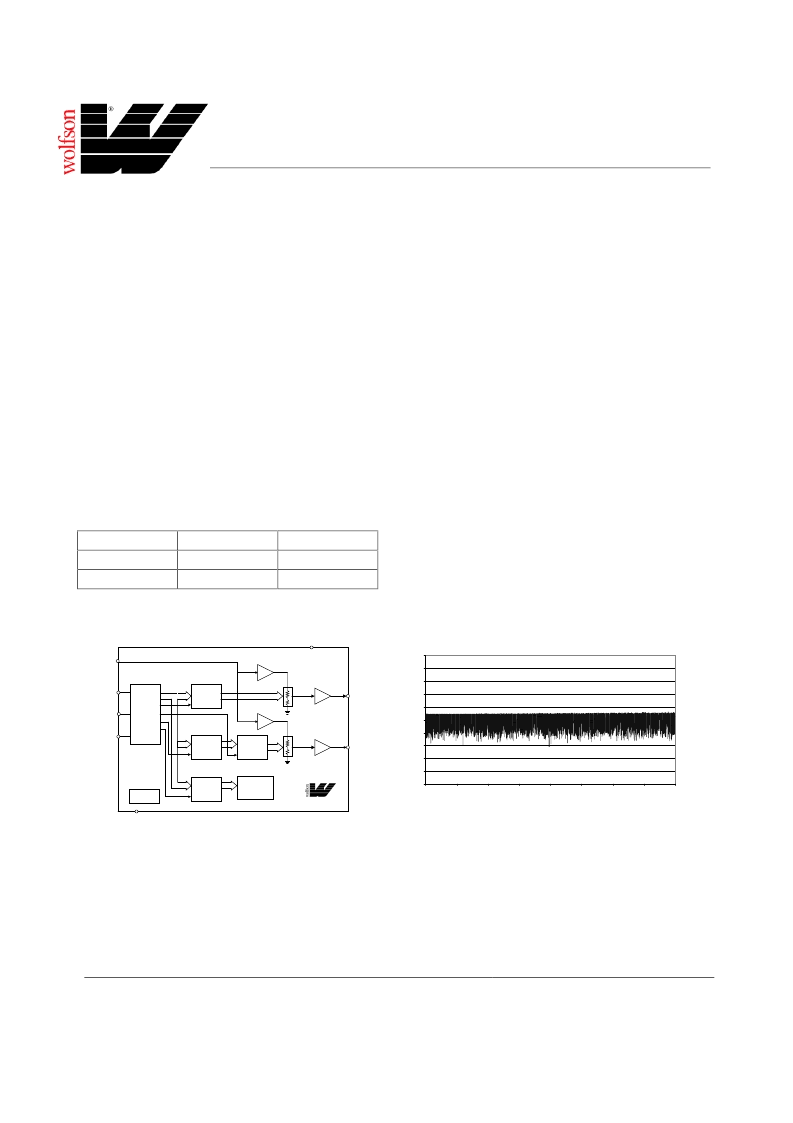
BLOCK DIAGRAM
TYPICAL PERFORMANCE
(7) OUTB
(4) OUTA
12-BIT
DAC B
HOLDING
LATCH
12-BIT
DAC A
LATCH
REFIN(6)
POWER-ON
RESET
DIN (1)
SCLK (2)
NCS (3)
(5)
AGND
VDD
(8)
POWERDOWN/
SPEED
CONTROL
12-BIT
DAC B
CONTROL
LATCH
DAC
OUTPUT
BUFFER
2-BIT
CONTROL
LATCH
X1
X1
X2
X2
DAC
OUTPUT
BUFFER
REFERENCE
INPUT BUFFER
REFERENCE
INPUT BUFFER
WM2618
16-BIT
SHIFT
REAND
CONTROL
LOGIC
data
5V = VDD, V
REF
= 2.048V, Speed = Fast mode, Load = 10k/100pF
-1
-0.8
-0.6
-0.4
-0.2
0
0.2
0.4
0.6
0.8
1
0
512
1024
1536
2048
2559
3071
3583
4095
DIGITAL CODE
D
相關(guān)PDF資料 |
PDF描述 |
|---|---|
| WM2618CD | Dual 12-Bit Serial Input Voltage Output DAC |
| WM2618ID | Connector assemblies, Network cables; |
| WM2623 | Low Power 8-bit Serial Input DAC |
| WM2623CD | Low Power 8-bit Serial Input DAC |
| WM2623ID | Low Power 8-bit Serial Input DAC |
相關(guān)代理商/技術(shù)參數(shù) |
參數(shù)描述 |
|---|---|
| WM2618CD | 制造商:WOLFSON 制造商全稱:WOLFSON 功能描述:Dual 12-Bit Serial Input Voltage Output DAC |
| WM2618ID | 制造商:WOLFSON 制造商全稱:WOLFSON 功能描述:Dual 12-Bit Serial Input Voltage Output DAC |
| WM2619 | 制造商:WOLFSON 制造商全稱:WOLFSON 功能描述:12-bit Parallel Input Voltage Output DAC |
| WM2619CDT | 制造商:WOLFSON 制造商全稱:WOLFSON 功能描述:12-bit Parallel Input Voltage Output DAC |
| WM2619IDT | 制造商:WOLFSON 制造商全稱:WOLFSON 功能描述:12-bit Parallel Input Voltage Output DAC |
發(fā)布緊急采購,3分鐘左右您將得到回復(fù)。