- 您現(xiàn)在的位置:買(mǎi)賣(mài)IC網(wǎng) > PDF目錄140365 > WF2M32U-90G2UQE5A (WHITE ELECTRONIC DESIGNS CORP) 2M X 32 FLASH 5V PROM MODULE, 90 ns, CQFP68 PDF資料下載
參數(shù)資料
| 型號(hào): | WF2M32U-90G2UQE5A |
| 廠商: | WHITE ELECTRONIC DESIGNS CORP |
| 元件分類: | PROM |
| 英文描述: | 2M X 32 FLASH 5V PROM MODULE, 90 ns, CQFP68 |
| 封裝: | 22.40 X 22.40 MM, 3.56 MM HEIGHT, HERMATIC SEALED, CERAMIC, QFP-68 |
| 文件頁(yè)數(shù): | 1/14頁(yè) |
| 文件大小: | 213K |
| 代理商: | WF2M32U-90G2UQE5A |
當(dāng)前第1頁(yè)第2頁(yè)第3頁(yè)第4頁(yè)第5頁(yè)第6頁(yè)第7頁(yè)第8頁(yè)第9頁(yè)第10頁(yè)第11頁(yè)第12頁(yè)第13頁(yè)第14頁(yè)
1
White Electronic Designs Corporation (602) 437-1520
White Electronic Designs
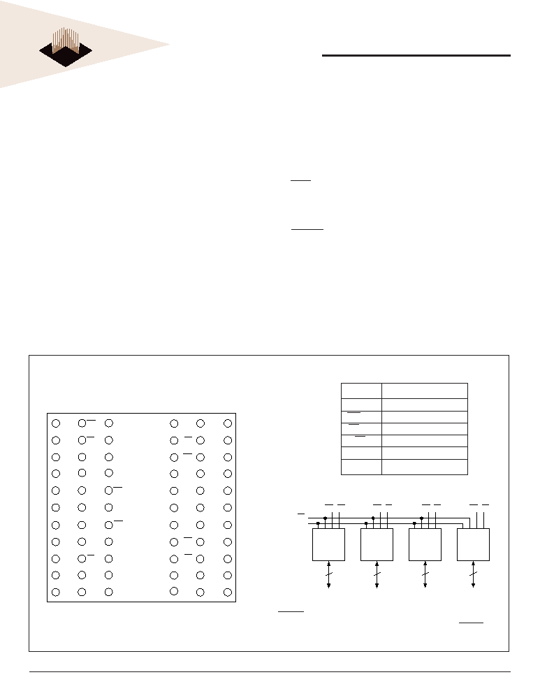
WF2M32-XXX5
FIG. 1 PIN CONFIGURATION FOR WF2M32-XHX5
PIN DESCRIPTION
I/O8
I/O9
I/O10
A14
A16
A11
A0
A18
I/O0
I/O1
I/O2
WE2
CS2
GND
I/O11
A10
A9
A15
VCC
CS1
A19
I/O3
I/O15
I/O14
I/O13
I/O12
OE
A17
WE1
I/O7
I/O6
I/O5
I/O4
I/O24
I/O25
I/O26
A7
A12
A20
A13
A8
I/O16
I/O17
I/O18
VCC
CS4
WE4
I/O27
A4
A5
A6
WE3
CS3
GND
I/O19
I/O31
I/O30
I/O29
I/O28
A1
A2
A3
I/O23
I/O22
I/O21
I/O20
11
22
33
44
55
66
1
12
23
34
45
56
TOP VIEW
BLOCKDIAGRAM
2M x 8
8
I/O 0-7
WE CS
1
2M x 8
8
I/O 8-15
WE CS
2
2M x 8
8
I/O 16-23
WE CS
3
2M x 8
8
I/O 24-31
WE CS
4
A 0- 20
OE
2Mx32 5V Flash Module
■
Commercial, Industrial, and Extended Tempera-
ture Ranges
■
5 Volt Read and Write. 5V ± 10% Supply.
■
Low Power CMOS
■
Data Polling and Toggle Bit feature for detection
of program or erase cycle completion.
■
Supports reading or programming data to a
sector not being erased.
■
RESET pin resets internal state machine to the
read mode.
■
Built in Decoupling Caps and Multiple Ground
Pins for Low Noise Operation, Separate Power
and Ground Planes to improve noise immunity
FEATURES
■
Access Time of 90, 120, 150ns
■
Packaging:
66 pin, PGA Type, 1.185" square, Hermetic
Ceramic HIP (Package 401).
68 lead, Hermetic CQFP (G2U), 22.4mm
(0.880") square (Package 510) 3.56mm
(0.140") height. Designed to fit JEDEC 68 lead
0.990" CQFJ footprint (Fig. 3)
■
Sector Architecture
32 equal size sectors of 64KBytes per each
2Mx8 chip
Any combination of sectors can be erased.
Also supports full chip erase.
■
Minimum 100,000 Write/Erase Cycles Minimum
■
Organized as 2Mx32
RESET internally tied to Vcc in the HIP package for this pin
configuration. See Alternate Pin Configuration with RESET tied
to pin 12 for system control of reset (Fig. 10, page 11).
December 2003 Rev.4
PRELIMINARY*
* This data sheet describes a product under development, not fully characterized,
and is subject to change without notice.
Note:
For programming information refer to Flash Programming 16M5 Application
Note.
I/O0-31
Data Inputs/Outputs
A0-20
Address Inputs
WE1-4
Write Enables
CS1-4
Chip Selects
OE
Output Enable
VCC
Power Supply
GND
Ground
相關(guān)PDF資料 |
PDF描述 |
|---|---|
| WV3HG32M72EER403AD6SG | 32M X 72 DDR DRAM MODULE, 0.6 ns, DMA240 |
| W3E16M72SR200BI | 16M X 72 DDR DRAM, 0.75 ns, PBGA219 |
| W764M32V100SBI | 64M X 32 FLASH 3V PROM, 100 ns, PBGA107 |
| W25Q16CLSSIG | 16M X 1 SPI BUS SERIAL EEPROM, PDSO8 |
| W25Q40BWUXIG | 4M X 1 SPI BUS SERIAL EEPROM, PDSO8 |
相關(guān)代理商/技術(shù)參數(shù) |
參數(shù)描述 |
|---|---|
| WF2M32-XG2UX5 | 制造商:未知廠家 制造商全稱:未知廠家 功能描述:Flash MCP |
| WF2M32-XHX5 | 制造商:未知廠家 制造商全稱:未知廠家 功能描述:Flash MCP |
| WF2M32-XXX5 | 制造商:WEDC 制造商全稱:White Electronic Designs Corporation 功能描述:2Mx32 5V Flash Module |
| WF-30 | 制造商:Stancor 功能描述: |
| WF300 | 制造商:未知廠家 制造商全稱:未知廠家 功能描述:DC to DC Converter |
發(fā)布緊急采購(gòu),3分鐘左右您將得到回復(fù)。