- 您現(xiàn)在的位置:買賣IC網(wǎng) > PDF目錄140354 > WEDPNF8M721V-1012BI (MICROSEMI CORP-PMG MICROELECTRONICS) SPECIALTY MEMORY CIRCUIT, PBGA275 PDF資料下載
參數(shù)資料
| 型號: | WEDPNF8M721V-1012BI |
| 廠商: | MICROSEMI CORP-PMG MICROELECTRONICS |
| 元件分類: | 存儲器 |
| 英文描述: | SPECIALTY MEMORY CIRCUIT, PBGA275 |
| 封裝: | 32 X 25 MM, PLASTIC, BGA-275 |
| 文件頁數(shù): | 15/42頁 |
| 文件大小: | 1297K |
| 代理商: | WEDPNF8M721V-1012BI |
第1頁第2頁第3頁第4頁第5頁第6頁第7頁第8頁第9頁第10頁第11頁第12頁第13頁第14頁當(dāng)前第15頁第16頁第17頁第18頁第19頁第20頁第21頁第22頁第23頁第24頁第25頁第26頁第27頁第28頁第29頁第30頁第31頁第32頁第33頁第34頁第35頁第36頁第37頁第38頁第39頁第40頁第41頁第42頁
22
White Electronic Designs Corporation Phoenix AZ (602) 437-1520
White Electronic Designs
WEDPNF8M721V-XBX
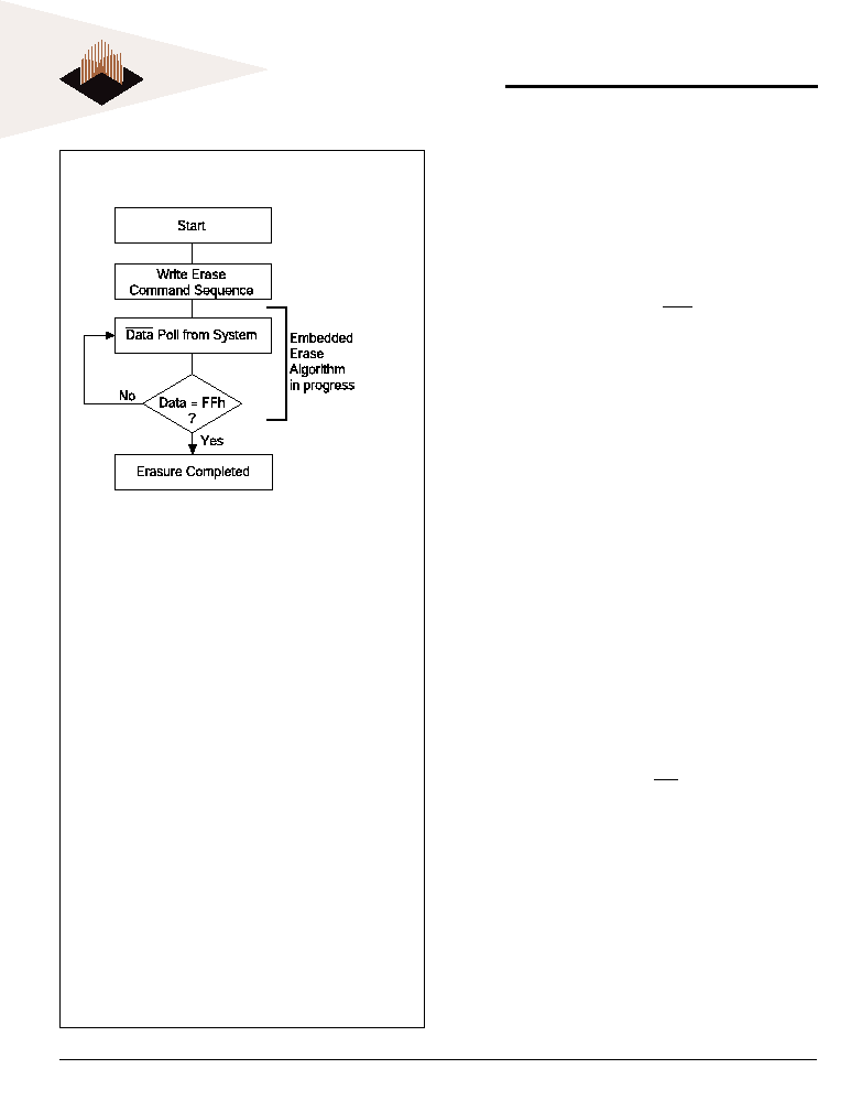
FIG. 7 ERASE OPERATION
1. See Table 5 for erase command sequence.
2. See "FD3 : Sector Erase Timer" for more information.
Any commands written to the device during the Embed-
ded Program Algorithm are ignored. Note that a
hardware
reset immediately terminates the programming operation.
The program command sequences should be reinitiated
once the device has reset to reading array data, to ensure
date integrity.
Programming is allowed in any sequence and across sector
boundaries.
A bit cannot be programmed from a 0
back to a 1. Attempting to do so may halt the operation
and set FD5 to “1”, or cause the Data Polling algorithm to
indicate the operation was successful. However, a succeed-
ing read will show that the data is still “0”. Only erase op-
erations can conver t a “0” to a “1”.
CHIP ERASE COMMAND SEQUENCE
Chip erase is six bus cycle operation. The chip erase com-
mand sequence is initiated by writing two unlock cycles,
followed by a setup command. Two additional unlock write
cycles are then followed by the chip erase command, which
in turn invokes the Embedded Erase algorithm. The device
does
not require the system to preprogram prior to erase.
The Embedded Erase algorithm automatically programs and
verifies the entire memory for an all zero data pattern prior
to electrical erase. The system is not required to provide
any controls or timings during these operations. Table 7
shows the address and data requirements for the chip erase
command sequence.
Any commands written to the chip during the Embedded
Erase algorithm are ignored. Note that a
hardware reset
during the chip erase operation immediately terminates the
operation. The Chip Erase command sequence should be
re-initiated once the device has returned to reading array
data, to ensure data integrity.
The system can determine the status of the erase operation
by using FD7, FD6, or FD2, or RY/BY1. See “Write Operation
Status” for information on these status bits. When the Em-
bedded Erase algorithm is complete, the device returns to
reading array data and addresses are no longer latched.
Figure 7 illustrates the algorithm for the erase operation. See
the Erase/Program Operations tables in “Flash AC Character-
istics” for parameters, and to Figure 13 for timings diagram.
SECTOR ERASE COMMAND
SEQUENCE
Sector erase is six bus cycle operation. The sector erase
command sequence is initiated by writing two unlock
cycles, followed by a setup command. Two additional un-
lock write cycles are then followed by the address of the
相關(guān)PDF資料 |
PDF描述 |
|---|---|
| WS512K16-35FLM | 512K X 16 MULTI DEVICE SRAM MODULE, 35 ns, CDFP44 |
| WS512K32NV-15G2UM | 512K X 32 MULTI DEVICE SRAM MODULE, 15 ns, CQFP68 |
| WS512K8-35CMEA | 512K X 8 MULTI DEVICE SRAM MODULE, 35 ns, CDMA32 |
| WF2M32-90G4TC | 8M X 8 FLASH 12V PROM MODULE, 90 ns, QMA68 |
| WED3DL644V10BC | 4M X 64 SYNCHRONOUS DRAM, 7 ns, PBGA153 |
相關(guān)代理商/技術(shù)參數(shù) |
參數(shù)描述 |
|---|---|
| WEDPNF8M721V-1012BM | 制造商:未知廠家 制造商全稱:未知廠家 功能描述:8Mx72 Synchronous DRAM + 8Mb Flash Mixed Module Multi-Chip Package |
| WEDPNF8M721V-1015BC | 制造商:未知廠家 制造商全稱:未知廠家 功能描述:8Mx72 Synchronous DRAM + 8Mb Flash Mixed Module Multi-Chip Package |
| WEDPNF8M721V-1015BI | 制造商:未知廠家 制造商全稱:未知廠家 功能描述:8Mx72 Synchronous DRAM + 8Mb Flash Mixed Module Multi-Chip Package |
| WEDPNF8M721V-1015BM | 制造商:未知廠家 制造商全稱:未知廠家 功能描述:8Mx72 Synchronous DRAM + 8Mb Flash Mixed Module Multi-Chip Package |
| WEDPNF8M721V-1210BC | 制造商:未知廠家 制造商全稱:未知廠家 功能描述:8Mx72 Synchronous DRAM + 8Mb Flash Mixed Module Multi-Chip Package |
發(fā)布緊急采購,3分鐘左右您將得到回復(fù)。