- 您現(xiàn)在的位置:買賣IC網 > PDF目錄245655 > WED9LC6816V1510BI (WHITE ELECTRONIC DESIGNS CORP) SPECIALTY MEMORY CIRCUIT, PBGA153 PDF資料下載
參數(shù)資料
| 型號: | WED9LC6816V1510BI |
| 廠商: | WHITE ELECTRONIC DESIGNS CORP |
| 元件分類: | 存儲器 |
| 英文描述: | SPECIALTY MEMORY CIRCUIT, PBGA153 |
| 封裝: | 14 X 22 MM, MO-163, BGA-153 |
| 文件頁數(shù): | 20/26頁 |
| 文件大?。?/td> | 324K |
| 代理商: | WED9LC6816V1510BI |
WED9LC6816V
3
White Electronic Designs Corporation (602) 437-1520 www.whiteedc.com
White Electronic Designs
September, 2003
Rev. 1
White Electronic Designs Corp. reserves the right to change products or specications without notice.
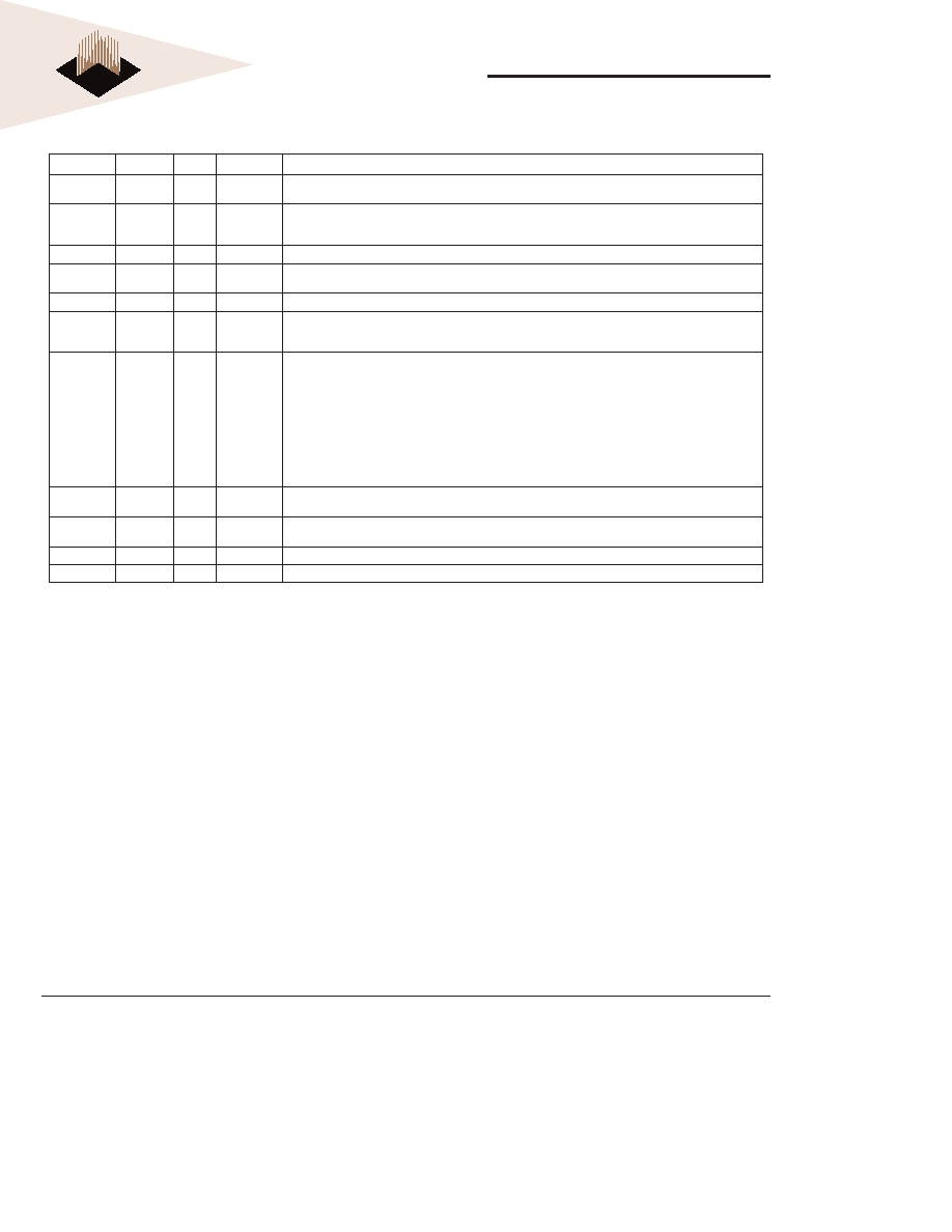
OUTPUT FUNCTIONAL DESCRIPTIONS
Symbol
Type
Signal
Polarity
Function
SSCK
Input
Pulse
Positive
Edge
The system clock input. All of the SSRAM inputs are sampled on the rising edge of the clock.
SSADS#
SSOE#
SSWE#
Input
Pulse
Active Low
When sampled at the positive rising edge of the clock, SSADS#, SSOE#, and SSWE# dene the
operation to be executed by the SSRAM.
SSCE#
Input
Pulse
Active Low
SSCE# disable or enable SSRAM device operation.
SDCK
Input
Pulse
Positive
Edge
The system clock input. All of the SDRAM inputs are sampled on the rising edge of the clock.
SDCE
Input
Pulse
Active Low
SDCE disable or enable device operation by masking or enabling all inputs except SDCK and BWE0
SDRAS#
SDCAS#
SDWE#
Input
Pulse
Active Low
When sampled at the positive rising edge of the clock, SDCAS#, SDRAS#, and SDWE# dene
the operation to be executed by the SDRAM.
A0-17,
SDA10
Input
Level
—
Address bus for SSRAM and SDRAM
A0 and A1 are the burst address inputs for the SSRAM
During a Bank Active command cycle, A0-11, SDA10 denes the row address (RA0-10) when sampled
at the rising clock edge.
During a Read or Write command cycle, A0-7 denes the column address (CA0-7) when sampled at
the rising clock edge. In addition to the row address, SDA10 is used to invoke autoprecharge operation
at the end of the Burst Read or Write Cycle. If SDA10 is high, autoprecharge is selected and A12 and
A13 dene the bank to be precharged. If SDA10 is low, autoprecharge is disabled.
During a Precharge command cycle, SDA10 is used in conjunction with A12 and A13 to control which
bank(s) to precharge. If SDA10 is high, all banks will be precharged regardless of the state of A12 and
A13. If SDA10 is low, then A12 and A13 are used to dene which bank to precharge.
DQ0-31
Input
Output
Level
—
Data Input/Output are multiplexed on the same pins.
BWE0-3
Input
Pulse
BWE0-3 perform the byte write enable function for the SSRAM and DQM function for the SDRAM.
BWE0 is associated with DQ0-7, BWE1 with DQ8-15, BWE2 with DQ16-23 and BWE3 with DQ24-31.
VCC, VSS
Supply
Power and ground for the input buffers and the core logic.
VCCQ
Supply
Data base power supply pins, 3.3V (2.5V future)
相關PDF資料 |
PDF描述 |
|---|---|
| WED3DG644V75D1I-SG | 4M X 64 SYNCHRONOUS DRAM MODULE, ZMA144 |
| WF-128K32-120HM | 512K X 8 FLASH 12V PROM MODULE, 120 ns, CPGA66 |
| WF128K32-200HM | 512K X 8 FLASH 12V PROM MODULE, 200 ns, CHIP66 |
| WMS512K8-120DEI | 512K X 8 STANDARD SRAM, 120 ns, CDSO32 |
| WMF2M8-150FLM5 | 2M X 8 FLASH 5V PROM, 150 ns, CDFP44 |
相關代理商/技術參數(shù) |
參數(shù)描述 |
|---|---|
| WED9LC6816V1512BC | 制造商:未知廠家 制造商全稱:未知廠家 功能描述:256K X 32 SSRAM/ 4M X 32 SDRAM |
| WED9LC6816V1512BI | 制造商:未知廠家 制造商全稱:未知廠家 功能描述:256K X 32 SSRAM/ 4M X 32 SDRAM |
| WED9LC6816V1610BC | 制造商:未知廠家 制造商全稱:未知廠家 功能描述:256K X 32 SSRAM/ 4M X 32 SDRAM |
| WED9LC6816V1610BI | 制造商:White Electronic Designs 功能描述:Res Thin Film 2010 196 Ohm 0.25% 1/4W ±10ppm/°C Molded SMD Plastic T/R 制造商:White Electronic Designs 功能描述:256KX32 SSRAM/ 4MX32 SDRAM |
| WED9LC6816V1612BC | 制造商:未知廠家 制造商全稱:未知廠家 功能描述:256K X 32 SSRAM/ 4M X 32 SDRAM |
發(fā)布緊急采購,3分鐘左右您將得到回復。