- 您現(xiàn)在的位置:買賣IC網(wǎng) > PDF目錄140379 > WE128K32-300G2TME (MICROSEMI CORP-PMG MICROELECTRONICS) 128K X 32 EEPROM 5V MODULE, 300 ns, CQFP68 PDF資料下載
參數(shù)資料
| 型號: | WE128K32-300G2TME |
| 廠商: | MICROSEMI CORP-PMG MICROELECTRONICS |
| 元件分類: | PROM |
| 英文描述: | 128K X 32 EEPROM 5V MODULE, 300 ns, CQFP68 |
| 封裝: | 22.40 X 22.40 MM, 4.57 MM HEIGHT, HERMETIC SEALED, CERAMIC, LQFP-68 |
| 文件頁數(shù): | 9/11頁 |
| 文件大小: | 161K |
| 代理商: | WE128K32-300G2TME |
7
White Electronic Designs Corporation Phoenix, AZ (602) 437-1520
WE128K32-XG2TXE
PAGE WRITE OPERATION
The WE128K32-XG2TXE has a page write operation that allows
one to 128 bytes of data to be written into the device and
consecutively loads during the internal programming period.
Successive bytes may be loaded in the same manner after the first
data byte has been loaded. An internal timer begins a time out
operation at each write cycle. If another write cycle is completed
within 30
cycle restarts the delay period. The write cycles can be continued
as long as the interval is less than the time out period.
The usual procedure is to increment the least significant
address lines from A0 through A6 at each write cycle. In this
manner a page of up to 128 bytes can be loaded in to the
EEPROM in a burst mode before beginning the relatively long
interval programming cycle.
After the 30
s time out is completed, the EEPROM begins an
internal write cycle. During this cycle the entire page of bytes
will be written at the same time. The internal programming
cycle is the same regardless of the number of bytes accessed.
PAGE WRITE CHARACTERISTICS
(VCC = 5.0V, VSS = 0V, TA = -55
°C to +125°C)
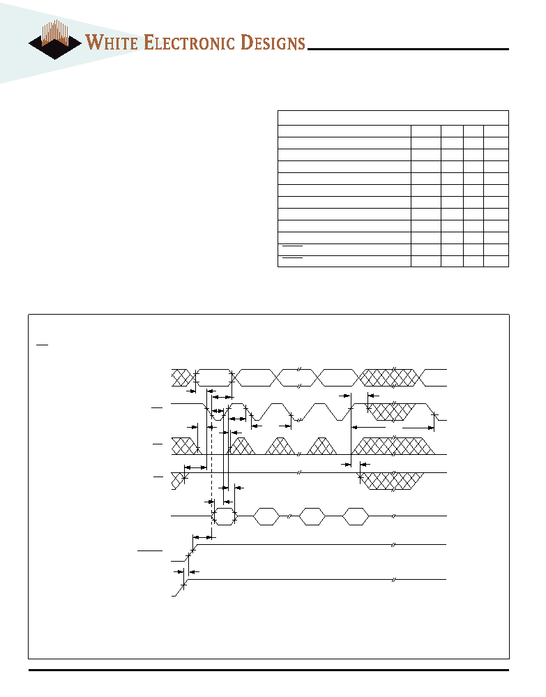
FIG. 7
PAGE WRITE WAVEFORMS
CS CONTROLLED(1)
1. This parameter is guarenteed by design but not tested.
Page Mode Write Characteristics
Parameter
Symbol
Min
Max
Unit
Write Cycle Time, TYP = 6ms
tWC
10
ms
Address Set-up Time
tAS
0ns
Address Hold Time
tAH
150
ns
Data Set-up Time
tDS
100
ns
Data Hold Time
tDH
10
ns
Write Pulse Width
tWP
250
ns
Byte Load Cycle Time (1)
tBLC
30
s
Byte Load Window (1)
tBL
100
s
Data Latch Time
tDL
300
ns
RESET Protect Time (1)
tRP
100
s
RESET High Time (1)
tRES
1
s
DATA IN
tCS
tCH
t OEH
tWP
tOES
tBLC
tAS
tAH
tBL
t WC
tDS
WE
tDL
OE
CS
RESET
Vcc
ADDRESS (2)
A0-16
tRES
tRP
tDH
NOTES:
1. tDF and tDFR are defined as the time at which the outputs achieve the
open circuit conditions and are no longer driven.
相關(guān)PDF資料 |
PDF描述 |
|---|---|
| WED7F112IDE33ADC25 | 7M X 16 FLASH 3.3V PROM, DMA144 |
| WED7G1G6IDE36ADC25 | 104M X 16 FLASH 3.3V PROM, DMA144 |
| WEDPS512K32-17BI | 512K X 32 MULTI DEVICE SRAM MODULE, 17 ns, PBGA143 |
| WF128K32-150G4TC5A | 128K X 32 FLASH 5V PROM MODULE, 150 ns, CQFP68 |
| WF128K32-70G4TQ5A | 128K X 32 FLASH 5V PROM MODULE, 70 ns, CQFP68 |
相關(guān)代理商/技術(shù)參數(shù) |
參數(shù)描述 |
|---|---|
| WE128K32-300G2TQ | 制造商:未知廠家 制造商全稱:未知廠家 功能描述:x32 EEPROM Module |
| WE128K32-300G2TQA | 制造商:未知廠家 制造商全稱:未知廠家 功能描述:x32 EEPROM Module |
| WE128K32-300G4C | 制造商:未知廠家 制造商全稱:未知廠家 功能描述:x32 EEPROM Module |
| WE128K32-300G4CA | 制造商:未知廠家 制造商全稱:未知廠家 功能描述:x32 EEPROM Module |
| WE128K32-300G4I | 制造商:未知廠家 制造商全稱:未知廠家 功能描述:x32 EEPROM Module |
發(fā)布緊急采購,3分鐘左右您將得到回復(fù)。