- 您現(xiàn)在的位置:買賣IC網(wǎng) > PDF目錄361798 > W921C400 Microcontroller PDF資料下載
參數(shù)資料
| 型號: | W921C400 |
| 英文描述: | Microcontroller |
| 中文描述: | 微控制器 |
| 文件頁數(shù): | 20/53頁 |
| 文件大小: | 394K |
| 代理商: | W921C400 |
第1頁第2頁第3頁第4頁第5頁第6頁第7頁第8頁第9頁第10頁第11頁第12頁第13頁第14頁第15頁第16頁第17頁第18頁第19頁當前第20頁第21頁第22頁第23頁第24頁第25頁第26頁第27頁第28頁第29頁第30頁第31頁第32頁第33頁第34頁第35頁第36頁第37頁第38頁第39頁第40頁第41頁第42頁第43頁第44頁第45頁第46頁第47頁第48頁第49頁第50頁第51頁第52頁第53頁
W921E400A/W921C400
- 20 -
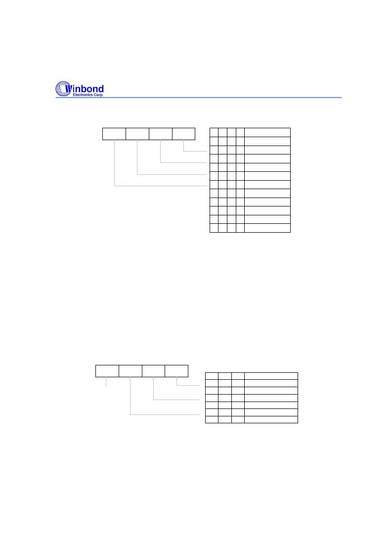
SRSPC register: (address = 00BH, default data = 0H)
b3
b2
b1
b0
b1 b0
Input frequency
0
0
0
1
1
0
1
1
fsys/4 Hz
fsys/8 Hz
fsys/16 Hz
b3 b2
0
0
0
0
0
0
0
0
0
1
0
1
0
1
0
1
1
0
0
0
0
1
1
0
1
1
1
1
0
0
0
0
0
1
1
0
fsys/32 Hz
fsys/64 Hz
fsys/128 Hz
fsys/256 Hz
fsys/512 Hz
fsys/1024 Hz
fsys/2048 Hz
Reserved
Normally the WCLK or RCLK pin will remain in high state and the serial data will be latched at the
rising edge of the WCLK or RCLK signal, but the serial clock inverter control register (SRINV) will
invert the above function. In this case WCLK or RCLK pin will remain in low state and the serial data
will be latched at the falling edge of the WCLK or RCLK signal.
The transmitting serial clock can come from WCLK or RCLK, depending on which one is enabled. If
the serial function is disabled, it will cause the relative pins to be in high impedance and it will not
affect the contents of serial buffer registers (start at address 050H).
6.7 DTMF Generator
There is one dual tone multi-frequency (DTMF) generator channel in this chip. The correct DTMF
output frequency is decided by the OSCCTR register as shown below.
OSCCTR register: (address = 013H, default data = 0H)
b3
b2
b1
b0
Reserved
b2
b1
b0
0
0
0
0
1
1
0
0
1
1
0
0
0
1
0
1
0
1
Osc. Selection
400 KHz
800 KHz
2 MHz
4 MHz
Reserved
3.58MHz
相關(guān)PDF資料 |
PDF描述 |
|---|---|
| W921C840 | Microcontroller |
| W921C880 | Microcontroller |
| W921E400A | 4-Bit Microcontroller(4位微控制器) |
| W921E400 | 4-Bit Microcontroller(4位微控制器) |
| W925C240 | Telephone Controller |
相關(guān)代理商/技術(shù)參數(shù) |
參數(shù)描述 |
|---|---|
| W921C840 | 制造商:未知廠家 制造商全稱:未知廠家 功能描述:Microcontroller |
| W921C880 | 制造商:未知廠家 制造商全稱:未知廠家 功能描述:Microcontroller |
| W921E400 | 制造商:WINBOND 制造商全稱:Winbond 功能描述:4-BIT MICROCONTROLLER |
| W921E400A | 制造商:WINBOND 制造商全稱:Winbond 功能描述:4-BIT MICROCONTROLLER |
| W921E840 | 制造商:WINBOND 制造商全稱:Winbond 功能描述:4-BIT MICROCONTROLLER |
發(fā)布緊急采購,3分鐘左右您將得到回復。