- 您現(xiàn)在的位置:買賣IC網(wǎng) > PDF目錄202143 > W3EG7266S202BD4IF (WHITE ELECTRONIC DESIGNS CORP) 64M X 72 DDR DRAM MODULE, 0.8 ns, DMA200 PDF資料下載
參數(shù)資料
| 型號(hào): | W3EG7266S202BD4IF |
| 廠商: | WHITE ELECTRONIC DESIGNS CORP |
| 元件分類: | DRAM |
| 英文描述: | 64M X 72 DDR DRAM MODULE, 0.8 ns, DMA200 |
| 封裝: | LEAD FREE, SO-DIMM-200 |
| 文件頁(yè)數(shù): | 11/13頁(yè) |
| 文件大小: | 191K |
| 代理商: | W3EG7266S202BD4IF |
第1頁(yè)第2頁(yè)第3頁(yè)第4頁(yè)第5頁(yè)第6頁(yè)第7頁(yè)第8頁(yè)第9頁(yè)第10頁(yè)當(dāng)前第11頁(yè)第12頁(yè)第13頁(yè)
W3EG7266S-AD4
-BD4
7
White Electronic Designs Corporation (602) 437-1520 www.wedc.com
White Electronic Designs
October 2004
Rev. 7
PRELIMINARY
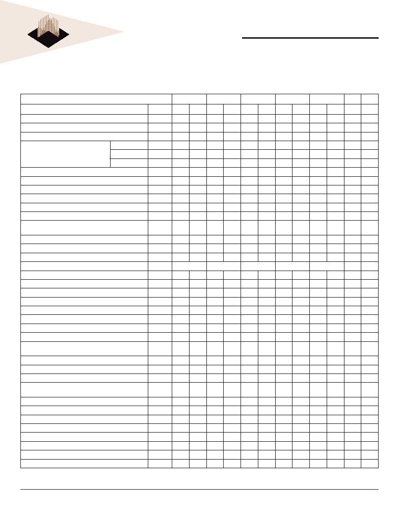
DDR SDRAM COMPONENT ELECTRICAL CHARACTERISTICS AND RECOMMENDED
AC OPERATING CONDITIONS
DDR400: VCC = VCCQ = +2.6V ± 0.1V
AC CHARACTERISTICS
403
335
262
265
202
PARAMETER
SYMBOL MIN
MAX
MIN
MAX
MIN
MAX
MIN
MAX
MIN
MAX UNITS NOTES
Access window of DQs from CK/CK#
tAC
-0.7
+0.7
-0.7
+0.7
-0.75 +0.75 -0.75
0.75
-0.8
0.8
ns
CK high-level width
tCH
0.45
0.55
0.45
0.55
0.45
0.55
0.45
0.55
0.45
0.55
tCK
25
CK low-level width
tCL
0.45
0.55
0.45
0.55
0.45
0.55
0.45
0.55
0.45
0.55
tCK
25
Clock cycle time
CL = 3
tCK (3)
5
7.5
6
13
7.5
13
7.5
13
8
13
ns
38, 43
CL = 2.5
tCK (2.5)
6
13
7.5
13
7.5
13
7.5/10
13
10
13
ns
38, 43
CL = 2
tCK (2)
7.5
13
ns
37, 42
DQ and DM input hold time relative to DQS
tDH
0.4
0.45
0.5
0.6
ns
22, 26
DQ and DM input setup time relative to DQS
tDS
0.4
0.45
0.5
0.6
ns
22, 26
DQ and DM input pulse width (for each input)
tDIPW
1.75
2
ns
26
Access window of DQS from CK/CK#
tDQSCK
-0.6
+0.6
-0.60 +0.60 -0.75 +0.75 +0.75
-0.8
+0.8
ns
DQS input high pulse width
tDQSH
0.35
tCK
DQS input low pulse width
tDQSL
0.35
tCK
DQS-DQ skew, DQS to last DQ valid, per group, per
access
tDQSQ
0.40
0.45
0.5
0.6
ns
22
Write command to rst DQS latching transition
tDQSS
0.72
1.28
0.75
1.25
0.75
1.25
0.75
1.25
0.75
1.25
tCK
DQS falling edge to CK rising - setup time
tDSS
0.2
tCK
DQS falling edge from CK rising - hold time
tDSH
0.2
tCK
Half clock period
tHP
tCH,tCL
ns
29
Data-out high-impedance window from CK/CK#
tHZ
+0.70
+0.75
+0.8
ns
16, 35
Data-out low-impedance window from CK/CK#
tLZ
-0.70
-0.75
-0.8
ns
16, 35
Address and control input hold time (1 V/ns)
tIHF
0.6
0.75
0.90
1.1
ns
12
ns
12
Address and control input setup time (1 V/ns)
tISF
0.6
0.75
0.90
1.1
ns
12
Address and control input hold time (0.5 V/ns)
tIHS
0.6
0.80
1
1.1
ns
12
Address and control input setup time (0.5 V/ns)
tISS
0.6
0.80
1
1.1
ns
12
Address and Control input pulse width (for each input)
tIPW
2.20
2.2
ns
LOAD MODE REGISTER command cycle time
tMRD
2
12151516
ns
DQ-DQS hold, DQS to rst DQ to go non-valid, per
access
tQH
tHP
- tQHS
tHP
- tQHS
tHP
- tQHS
tHP
- tQHS
tHP
- tQHS
ns
22
tQHS
0.50
0.60
0.75
1
ns
ACTIVE to PRECHARGE command
tRAS
40
70,000
42
70,000
40
120,000
40
120,000
40
120,000
ns
30
ACTIVE to READ with Auto precharge command
tRAP
15
20
ns
ACTIVE to ACTIVE/AUTO REFRESH command
period
tRC
55
60
65
70
ns
AUTO REFRESH command period
tRFC
70
72
75
72
75
ns
41
ACTIVE to READ or WRITE delay
tRCD
15
20
ns
PRECHARGE command period
tRP
15
20
ns
DQS read preamble
tRPRE
0.9
1.1
0.9
1.1
0.9
1.1
0.9
1.1
0.9
1.1
tCK
36
DQS read postamble
tRPST
0.4
0.6
0.4
0.6
0.4
0.6
0.4
0.6
0.4
0.6
tCK
36
ACTIVE bank a to ACTIVE bank b command
tRRD
10
12
15
ns
DQS write preamble
tWPRE
0.25
tCK
DQS write preamble setup time
tWPRES
00000
ns
17, 19
相關(guān)PDF資料 |
PDF描述 |
|---|---|
| WV3HG264M72EEU534D4-SG | 128M X 72 DDR DRAM MODULE, 0.5 ns, DMA200 |
| WE32K32N-120G2UCA | EEPROM 5V MODULE, CQFP68 |
| WED3DG6335V7D2 | 32M X 64 SYNCHRONOUS DRAM MODULE, DMA168 |
| ZZ1EEB050Z | 1 FUNCTIONS, 400 V, 5 A, DATA LINE FILTER |
| ZZ1EEB332H | 1 FUNCTIONS, 400 V, 5 A, DATA LINE FILTER |
相關(guān)代理商/技術(shù)參數(shù) |
參數(shù)描述 |
|---|---|
| W3EG7266S202D3 | 制造商:WEDC 制造商全稱:White Electronic Designs Corporation 功能描述:512MB - 64Mx72 DDR SDRAM REGISTERED w/PLL |
| W3EG7266S262AD4 | 制造商:WEDC 制造商全稱:White Electronic Designs Corporation 功能描述:512MB - 64Mx72 DDR SDRAM UNBUFFERED ECC w/PLL |
| W3EG7266S262AD4I | 制造商:WEDC 制造商全稱:White Electronic Designs Corporation 功能描述:512MB - 64Mx72 DDR SDRAM UNBUFFERED ECC w/PLL |
| W3EG7266S262BD4 | 制造商:WEDC 制造商全稱:White Electronic Designs Corporation 功能描述:512MB - 64Mx72 DDR SDRAM UNBUFFERED ECC w/PLL |
| W3EG7266S262BD4I | 制造商:WEDC 制造商全稱:White Electronic Designs Corporation 功能描述:512MB - 64Mx72 DDR SDRAM UNBUFFERED ECC w/PLL |
發(fā)布緊急采購(gòu),3分鐘左右您將得到回復(fù)。