- 您現(xiàn)在的位置:買賣IC網(wǎng) > PDF目錄68427 > W25Q16CLSFIG (WINBOND ELECTRONICS CORP) 16M X 1 SPI BUS SERIAL EEPROM, PDSO16 PDF資料下載
參數(shù)資料
| 型號(hào): | W25Q16CLSFIG |
| 廠商: | WINBOND ELECTRONICS CORP |
| 元件分類: | PROM |
| 英文描述: | 16M X 1 SPI BUS SERIAL EEPROM, PDSO16 |
| 封裝: | 0.300 INCH, GREEN, PLASTIC, SOIC-16 |
| 文件頁(yè)數(shù): | 55/77頁(yè) |
| 文件大?。?/td> | 2458K |
| 代理商: | W25Q16CLSFIG |
第1頁(yè)第2頁(yè)第3頁(yè)第4頁(yè)第5頁(yè)第6頁(yè)第7頁(yè)第8頁(yè)第9頁(yè)第10頁(yè)第11頁(yè)第12頁(yè)第13頁(yè)第14頁(yè)第15頁(yè)第16頁(yè)第17頁(yè)第18頁(yè)第19頁(yè)第20頁(yè)第21頁(yè)第22頁(yè)第23頁(yè)第24頁(yè)第25頁(yè)第26頁(yè)第27頁(yè)第28頁(yè)第29頁(yè)第30頁(yè)第31頁(yè)第32頁(yè)第33頁(yè)第34頁(yè)第35頁(yè)第36頁(yè)第37頁(yè)第38頁(yè)第39頁(yè)第40頁(yè)第41頁(yè)第42頁(yè)第43頁(yè)第44頁(yè)第45頁(yè)第46頁(yè)第47頁(yè)第48頁(yè)第49頁(yè)第50頁(yè)第51頁(yè)第52頁(yè)第53頁(yè)第54頁(yè)當(dāng)前第55頁(yè)第56頁(yè)第57頁(yè)第58頁(yè)第59頁(yè)第60頁(yè)第61頁(yè)第62頁(yè)第63頁(yè)第64頁(yè)第65頁(yè)第66頁(yè)第67頁(yè)第68頁(yè)第69頁(yè)第70頁(yè)第71頁(yè)第72頁(yè)第73頁(yè)第74頁(yè)第75頁(yè)第76頁(yè)第77頁(yè)
W25Q16CL
Publication Release Date: July 08, 2010
- 59 -
Preliminary - Revision A
11.2.37 Erase Security Registers (44h)
The W25Q16CL offers three 256-byte Security Registers which can be erased and programmed
individually. These registers may be used by the system manufacturers to store security and other
important information separately from the main memory array.
The Erase Security Register instruction is similar to the Sector Erase instruction. A Write Enable
instruction must be executed before the device will accept the Erase Security Register Instruction (Status
Register bit WEL must equal 1). The instruction is initiated by driving the /CS pin low and shifting the
instruction code “44h” followed by a 24-bit address (A23-A0) to erase one of the three security registers.
ADDRESS
A23-16
A15-12
A11-8
A7-0
Security Register #1
00h
0 0 0 1
0 0 0 0
Don’t Care
Security Register #2
00h
0 0 1 0
0 0 0 0
Don’t Care
Security Register #3
00h
0 0 1 1
0 0 0 0
Don’t Care
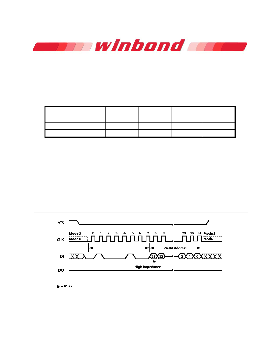
The Erase Security Register instruction sequence is shown in figure 35. The /CS pin must be driven high
after the eighth bit of the last byte has been latched. If this is not done the instruction will not be executed.
After /CS is driven high, the self-timed Erase Security Register operation will commence for a time
duration of tSE (See AC Characteristics). While the Erase Security Register cycle is in progress, the Read
Status Register instruction may still be accessed for checking the status of the BUSY bit. The BUSY bit is
a 1 during the erase cycle and becomes a 0 when the cycle is finished and the device is ready to accept
other instructions again. After the Erase Security Register cycle has finished the Write Enable Latch
(WEL) bit in the Status Register is cleared to 0. The Security Register Lock Bits LB[3:1] in the Status
Register-2 can be used to OTP protect the security registers. Once a lock bit is set to 1, the
corresponding security register will be permanently locked, Erase Security Register instruction to that
register will be ignored (See 11.1.9 for detail descriptions).
Figure 35. Erase Security Registers Instruction Sequence
Instruction (44h)
相關(guān)PDF資料 |
PDF描述 |
|---|---|
| W25Q16CVSSIG | 16M X 1 SPI BUS SERIAL EEPROM, PDSO8 |
| W25Q16DWZPIP | 16M X 1 SPI BUS SERIAL EEPROM, PDSO8 |
| W25Q20BWUXIP | 2M X 1 SPI BUS SERIAL EEPROM, PDSO8 |
| W25Q32BVSSAG | 32M X 1 SPI BUS SERIAL EEPROM, PDSO8 |
| W25Q32BVSSAP | 32M X 1 SPI BUS SERIAL EEPROM, PDSO8 |
相關(guān)代理商/技術(shù)參數(shù) |
參數(shù)描述 |
|---|---|
| W25Q16CLSFIP | 制造商:WINBOND 制造商全稱:Winbond 功能描述:2.5V 16M-BIT SERIAL FLASH MEMORY WITH DUAL AND QUAD SPI |
| W25Q16CLSNIG | 制造商:WINBOND 制造商全稱:Winbond 功能描述:2.5V 16M-BIT SERIAL FLASH MEMORY WITH DUAL AND QUAD SPI |
| W25Q16CLSNIP | 制造商:WINBOND 制造商全稱:Winbond 功能描述:2.5V 16M-BIT SERIAL FLASH MEMORY WITH DUAL AND QUAD SPI |
| W25Q16CLSSIG | 制造商:WINBOND 制造商全稱:Winbond 功能描述:2.5V 16M-BIT SERIAL FLASH MEMORY WITH DUAL AND QUAD SPI |
| W25Q16CLSSIP | 制造商:WINBOND 制造商全稱:Winbond 功能描述:2.5V 16M-BIT SERIAL FLASH MEMORY WITH DUAL AND QUAD SPI |
發(fā)布緊急采購(gòu),3分鐘左右您將得到回復(fù)。