- 您現(xiàn)在的位置:買賣IC網(wǎng) > PDF目錄359410 > VP510 (Zarlink Semiconductor Inc.) Bi Directional Colour Space Converter PDF資料下載
參數(shù)資料
| 型號: | VP510 |
| 廠商: | Zarlink Semiconductor Inc. |
| 英文描述: | Bi Directional Colour Space Converter |
| 中文描述: | 雙向定向色彩空間轉(zhuǎn)換 |
| 文件頁數(shù): | 6/14頁 |
| 文件大小: | 312K |
| 代理商: | VP510 |
VP 510
5
MAX
27 MHz
20ns
20ns
20ns
SYMBOL
Ts
Th
Tss
Trs
Trh
Thd
Trd
Tcd
Trd
Trd
DELAYED
HREF O/P
INPUT
CLOCK
INPUT
CLOCK
LUM
OUTPUT
Second I/P
Ts
Th
First I/P
LUM
INPUT
Tss
HREF
INPUT
First V or Q or Cb
Ts
Th
First U or I or Cr
CHROM
INPUT
CRI
Trh
Trs
CRO
Thd
First O/P Valid
Tcd
Second O/P Valid
First U or I or Cr Valid
Tcd
CHROM
O/P
FirstV or Q or CB Valid
Tcd
Tcd
MIN
DC
10ns
0ns
10ns
10ns
0ns
CHARACTERISTIC
I/P Clock Rate
I/P Set Up Time
I/P Hold Time
HREF Set Up Time
CREF Set Up Time
CREF Hold Time
Delayed HREF O/P Delay
CREF O/P Delay
Data O/P Delay
First O/P
Tcd
Thd
Second I/P
Tss
Ts
Th
First I/P
INPUT
CLOCK
RGB
INPUT
HREF
INPUT
DELAYED
HREF O/P
RGB
OUTPUT
CHARACTERISTIC
I/P Clock rate
I/P Set Up Time
I/P Hold Time
HREF Set Up Time
Delayed HREF O/P Delay
RGB O/P Delay
SYMBOL
Ts
Th
Tss
Thd
Tcd
MIN
DC
10ns
0ns
10ns
MAX
27MHz
20ns
20ns
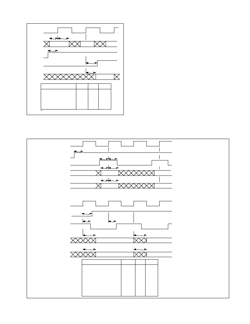
RGB data must normally be gamma corrected by the RAM's
before colour space conversion.
LUMINANCE AND CHROMINANCE
INPUTS
The 16 bit luminance and chrominance values must meet
the set up and hold times, with respect to the rising edge of the
clock, which are specified in Figure 7. Since the input rate will
be half the clock rate an additional signal is required to indicate
alternate clock periods. This signal ( CRI ) must also meet the
set up and hold requirements given in Figure 7. On the first
occurrence of CRI after HREF goes inactive ( High ), the 16 bit
input bus must contain the first 8 bit luminance component
plus the first 8 bit U,I, or Cr component, if the delay to the first
correctly filtered output is to match the fixed pipeline delay to
the HDLY and FO outputs. On the second occurrence it must
contain the second luminance component plus the first V, Q,
or Cb component. When HREF goes low the outputs will be
forced low after the 39 clock pipeline delay.
YUV or YIQ data is directly applied to the interpolating
filters by setting the BYPASS Bit in the Control Register. When
Y Cr Cb data is to be used this bit should be reset, and the
inputs will then be applied to the ranging and offset circuitry.
The SEL bit in the Control Register is used to determine the
ranging options. If this bit is reset then the Y input will be
Figure 6. RGB I/O Timing (Advanced Data)
Figure 7. Chrominance I/O Timing (Advanced Data)
相關PDF資料 |
PDF描述 |
|---|---|
| VP510CGGPFR | Bi Directional Colour Space Converter |
| VP520CGGGWR | Video Converter Circuit |
| VP520CGGH1R | Video Converter Circuit |
| VP520SCGGH1R | PAL/NTSC to CIF/QCIF Converter |
| VP520SCG | PAL/NTSC to CIF/QCIF Converter |
相關代理商/技術參數(shù) |
參數(shù)描述 |
|---|---|
| VP510CGGPFR | 制造商:ZARLINK 制造商全稱:Zarlink Semiconductor Inc 功能描述:Bi Directional Colour Space Converter |
| VP511 | 制造商:Platt Luggage 功能描述:Vacuum Pack |
| VP5-1200 | 制造商:COOPER BUSSMANN 功能描述:Ind General Purpose 76.8uH 30% Ferrite 2.08A Bulk |
| VP5-1200-R | 功能描述:固定電感器 76.8uH 0.2A 0.047ohms RoHS:否 制造商:AVX 電感:10 uH 容差:20 % 最大直流電流:1 A 最大直流電阻:0.075 Ohms 工作溫度范圍:- 40 C to + 85 C 自諧振頻率:38 MHz Q 最小值:40 尺寸:4.45 mm W x 6.6 mm L x 2.92 mm H 屏蔽:Shielded 端接類型:SMD/SMT 封裝 / 箱體:6.6 mm x 4.45 mm |
| VP5-1200TR | 制造商:COOPER BUSSMANN 功能描述:Ind Power Wirewound 76.8uH 30% Ferrite 2.08A T/R |
發(fā)布緊急采購,3分鐘左右您將得到回復。