- 您現(xiàn)在的位置:買賣IC網(wǎng) > PDF目錄361603 > UTC571 (友順科技股份有限公司) COMPANDER Complete compressor and expandor in one IChip PDF資料下載
參數(shù)資料
| 型號: | UTC571 |
| 廠商: | 友順科技股份有限公司 |
| 英文描述: | COMPANDER Complete compressor and expandor in one IChip |
| 中文描述: | 擴(kuò)展器完整的壓縮機(jī)和expandor一個(gè)IChip |
| 文件頁數(shù): | 9/14頁 |
| 文件大小: | 161K |
| 代理商: | UTC571 |
UTC571
LINEAR INTEGRATED CIRCUIT
YOUWANG ELECTRONICS CO.LTD
9
At very low input signal levels the bias current of Q 2 , (typically 50nA), will become significant as it must be
supplied by Q 5 . Another low level error can be caused by DC coupling into the rectifier. If an offset voltage exists
between the V IN input pin and the base of Q 2 , an error current of V
OS
/R 1 will be generated. A mere 1mV of
offset will cause an input current of 100nA which will produce twice the error of the input bias current. For highest
accuracy, the rectifier should be coupled into capacitively. At high input levels the
β
of the PNP Q 6 will begin to
suffer, and there will be an increasing error until the circuit saturates. Saturation can be avoided by limiting the
current into the rectifier input to 25
0
mA. If necessary, an external resistor may be placed in series with R 1 to limit
the current to this value. Figure 7 shows the rectifier accuracy vs input level at a frequency of 1kHz.
0
+1
-1
-40
-20
0
RECTIFIER INPUT dBm
E
Figure 7. Rectifier Accuracy
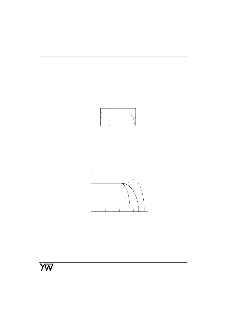
At very high frequencies, the response of the rectifier will fall off. The roll-off will be more pronounced at lower
input levels due to the increasing amount of gain required to switch between Q 5 or Q 6 conducting. The rectifier
frequency response for input levels of 0dBm, -20dBm, and -40dBm is shown in Figure 8. The response at all three
levels is flat to well above the audio range.
0
3
10K
1MEG
-40dBm
-20dBm
INPUT=0dBm
FREQUENCY(Hz)
G
Figure 8. Simplified
G Cell Schematic
相關(guān)PDF資料 |
PDF描述 |
|---|---|
| UTC7106 | 3/12 DIGIT,LCD DISPLAY A/D CONVERTERS |
| UTC75185 | LINEAR INTEGRATED CIRCUIT |
| UTC75323 | LINEAR INTEGRATED CIRCUIT |
| UTC7642 | ONE CHIP AM RADIO CIRCUIT |
| UTC78D | LINEAR INTEGRATED CIRCUIT |
相關(guān)代理商/技術(shù)參數(shù) |
參數(shù)描述 |
|---|---|
| UTC571N | 制造商:UTC-IC 制造商全稱:UTC-IC 功能描述:COMPANDER |
| UTC571NG-S16-R | 制造商:UTC-IC 制造商全稱:UTC-IC 功能描述:COMPANDER |
| UTC571NG-S16-T | 制造商:UTC-IC 制造商全稱:UTC-IC 功能描述:COMPANDER |
| UTC571NG-S16W-R | 制造商:UTC-IC 制造商全稱:UTC-IC 功能描述:COMPANDER |
| UTC571NG-S16W-T | 制造商:UTC-IC 制造商全稱:UTC-IC 功能描述:COMPANDER |
發(fā)布緊急采購,3分鐘左右您將得到回復(fù)。