- 您現(xiàn)在的位置:買賣IC網(wǎng) > PDF目錄300064 > UPD78053GC-XXX-8BT 8-BIT, MROM, 5 MHz, MICROCONTROLLER, PQFP80 PDF資料下載
參數(shù)資料
| 型號: | UPD78053GC-XXX-8BT |
| 元件分類: | 微控制器/微處理器 |
| 英文描述: | 8-BIT, MROM, 5 MHz, MICROCONTROLLER, PQFP80 |
| 封裝: | 14 X 14 MM, 1.40 MM PITCH, PLASTIC, QFP-80 |
| 文件頁數(shù): | 107/237頁 |
| 文件大小: | 2394K |
| 代理商: | UPD78053GC-XXX-8BT |
第1頁第2頁第3頁第4頁第5頁第6頁第7頁第8頁第9頁第10頁第11頁第12頁第13頁第14頁第15頁第16頁第17頁第18頁第19頁第20頁第21頁第22頁第23頁第24頁第25頁第26頁第27頁第28頁第29頁第30頁第31頁第32頁第33頁第34頁第35頁第36頁第37頁第38頁第39頁第40頁第41頁第42頁第43頁第44頁第45頁第46頁第47頁第48頁第49頁第50頁第51頁第52頁第53頁第54頁第55頁第56頁第57頁第58頁第59頁第60頁第61頁第62頁第63頁第64頁第65頁第66頁第67頁第68頁第69頁第70頁第71頁第72頁第73頁第74頁第75頁第76頁第77頁第78頁第79頁第80頁第81頁第82頁第83頁第84頁第85頁第86頁第87頁第88頁第89頁第90頁第91頁第92頁第93頁第94頁第95頁第96頁第97頁第98頁第99頁第100頁第101頁第102頁第103頁第104頁第105頁第106頁當(dāng)前第107頁第108頁第109頁第110頁第111頁第112頁第113頁第114頁第115頁第116頁第117頁第118頁第119頁第120頁第121頁第122頁第123頁第124頁第125頁第126頁第127頁第128頁第129頁第130頁第131頁第132頁第133頁第134頁第135頁第136頁第137頁第138頁第139頁第140頁第141頁第142頁第143頁第144頁第145頁第146頁第147頁第148頁第149頁第150頁第151頁第152頁第153頁第154頁第155頁第156頁第157頁第158頁第159頁第160頁第161頁第162頁第163頁第164頁第165頁第166頁第167頁第168頁第169頁第170頁第171頁第172頁第173頁第174頁第175頁第176頁第177頁第178頁第179頁第180頁第181頁第182頁第183頁第184頁第185頁第186頁第187頁第188頁第189頁第190頁第191頁第192頁第193頁第194頁第195頁第196頁第197頁第198頁第199頁第200頁第201頁第202頁第203頁第204頁第205頁第206頁第207頁第208頁第209頁第210頁第211頁第212頁第213頁第214頁第215頁第216頁第217頁第218頁第219頁第220頁第221頁第222頁第223頁第224頁第225頁第226頁第227頁第228頁第229頁第230頁第231頁第232頁第233頁第234頁第235頁第236頁第237頁
193
CHAPTER 8
16-BIT TIMER/EVENT COUNTER
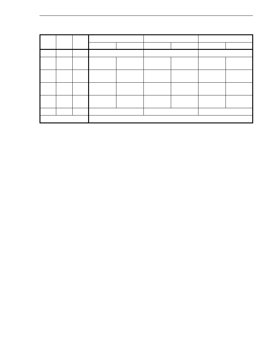
Table 8-6. 16-Bit Timer/Event Counter Interval Times
Minimum Interval Time
Maximum Interval Time
Resolution
MCS = 1
MCS = 0
MCS = 1
MCS = 0
MCS = 1
MCS = 0
000
2
× TI00 input cycle
216
× TI00 input cycle
TI00 input edge cycle
0
1
Setting
2
× 1/fX
Setting
216
× 1/fX
Setting
1/fX
prohibited
(400 ns)
prohibited
(13.1 ms)
prohibited
(200 ns)
010
2
× 1/fX
22
× 1/fX
216
× 1/fX
217
× 1/fX
1/fX
2
× 1/fX
(400 ns)
(800 ns)
(13.1 ms)
(26.2 ms)
(200 ns)
(400 ns)
011
22
× 1/fX
23
× 1/fX
217
× 1/fX
218
× 1/fX
2
× 1/fX
22
× 1/fX
(800 ns)
(1.6
s)
(26.2 ms)
(52.4 ms)
(400 ns)
(800 ns)
100
23
× 1/fX
24
× 1/fX
218
× 1/fX
219
× 1/fX
22
× 1/fX
23
× 1/fX
(1.6
s)
(3.2
s)
(52.4 ms)
(104.9 ms)
(800 ns)
(1.6
s)
111
2
× watch timer output cycle
216
× watch timer output cycle Watch timer output edge cycle
Other than above
Setting prohibited
Remarks 1. fX
: Main system clock oscillation frequency
2. MCS
: Bit 0 of oscillation mode selection register (OSMS)
3. TCL04 to TCL06 : Bits 4 to 6 of timer clock select register 0 (TCL0)
4. Figures in parentheses apply to operation with fX = 5.0 MHz
8.5.2 PWM output operations
Setting the 16-bit timer mode control register (TMC0), capture/compare control register 0 (CRC0), and the 16-bit
timer output control register (TOC0) as shown in Figure 8-13 allows operation as PWM output. Pulses with the duty
rate determined by the value set in 16-bit capture/compare register 00 (CR00) beforehand are output from the TO0/
P30 pin.
Set the active level width of the PWM pulse to the high-order 14 bits of CR00. Select the active level with bit 1
(TOC01) of the 16- bit timer output control register (TOC0).
This PWM pulse has a 14-bit resolution. The pulse can be converted to an analog voltage by integrating it with
an external low-pass filter (LPF). The PWM pulse is formed by a combination of the basic cycle determined by 28/
Φ and the sub-cycle determined by 214/Φ so that the time constant of the external LPF can be shortened. Count clock
Φ can be selected with bits 4 to 6 (TCL04 to TCL06) of the timer clock select register 0 (TCL0).
PWM output enable/disable can be selected with bit 0 (TOE0) of TOC0.
Cautions 1. PWM operation mode should be selected before setting CR00.
2. Be sure to write 0 to bits 0 and 1 of CR00.
3. Do not select PWM operation mode for external clock input from the TI00/P00/INTP0 pin.
TCL06
TCL05
TCL04
相關(guān)PDF資料 |
PDF描述 |
|---|---|
| UPD78322GJ-XXX-5BJ | 16-BIT, MROM, 16 MHz, MICROCONTROLLER, PQFP74 |
| UPD789132GS-XXX | 8-BIT, MROM, MICROCONTROLLER, PDSO30 |
| UPD789122UC-XXX-5A4 | 8-BIT, MROM, MICROCONTROLLER, PDSO30 |
| UPL4-NM-150 | INTERCONNECTION DEVICE |
| USB-AM-S-F-W-SM1-TR | 4 CONTACT(S), FEMALE, RIGHT ANGLE TELECOM AND DATACOM CONNECTOR, SURFACE MOUNT |
相關(guān)代理商/技術(shù)參數(shù) |
參數(shù)描述 |
|---|---|
| UPD78063GF-144-3BA | 制造商:World Products 功能描述: |
| UPD78063GF-147-3BA | 制造商:Renesas Electronics Corporation 功能描述: |
| UPD78063GF-169-3BA | 制造商:Renesas Electronics Corporation 功能描述: |
| UPD78064GF-132-3BA | 制造商:Renesas Electronics Corporation 功能描述: |
| UPD78070AGF-3BA-A | 制造商:Renesas Electronics Corporation 功能描述:MCU 8-bit 78K 78K0 CISC ROMLess 3.3V/5V 100-Pin PQFP |
發(fā)布緊急采購,3分鐘左右您將得到回復(fù)。