- 您現(xiàn)在的位置:買(mǎi)賣(mài)IC網(wǎng) > PDF目錄300064 > UPD780023AGK-xxx-9ET (NEC Corp.) Circular Connector; No. of Contacts:56; Series:MS27467; Body Material:Aluminum; Connecting Termination:Crimp; Connector Shell Size:25; Circular Contact Gender:Pin; Circular Shell Style:Straight Plug; Insert Arrangement:25-4 RoHS Compliant: No PDF資料下載
參數(shù)資料
| 型號(hào): | UPD780023AGK-xxx-9ET |
| 廠商: | NEC Corp. |
| 元件分類(lèi): | 圓形連接器 |
| 英文描述: | Circular Connector; No. of Contacts:56; Series:MS27467; Body Material:Aluminum; Connecting Termination:Crimp; Connector Shell Size:25; Circular Contact Gender:Pin; Circular Shell Style:Straight Plug; Insert Arrangement:25-4 RoHS Compliant: No |
| 中文描述: | 8位單晶片微控制器 |
| 文件頁(yè)數(shù): | 35/96頁(yè) |
| 文件大小: | 661K |
| 代理商: | UPD780023AGK-XXX-9ET |
第1頁(yè)第2頁(yè)第3頁(yè)第4頁(yè)第5頁(yè)第6頁(yè)第7頁(yè)第8頁(yè)第9頁(yè)第10頁(yè)第11頁(yè)第12頁(yè)第13頁(yè)第14頁(yè)第15頁(yè)第16頁(yè)第17頁(yè)第18頁(yè)第19頁(yè)第20頁(yè)第21頁(yè)第22頁(yè)第23頁(yè)第24頁(yè)第25頁(yè)第26頁(yè)第27頁(yè)第28頁(yè)第29頁(yè)第30頁(yè)第31頁(yè)第32頁(yè)第33頁(yè)第34頁(yè)當(dāng)前第35頁(yè)第36頁(yè)第37頁(yè)第38頁(yè)第39頁(yè)第40頁(yè)第41頁(yè)第42頁(yè)第43頁(yè)第44頁(yè)第45頁(yè)第46頁(yè)第47頁(yè)第48頁(yè)第49頁(yè)第50頁(yè)第51頁(yè)第52頁(yè)第53頁(yè)第54頁(yè)第55頁(yè)第56頁(yè)第57頁(yè)第58頁(yè)第59頁(yè)第60頁(yè)第61頁(yè)第62頁(yè)第63頁(yè)第64頁(yè)第65頁(yè)第66頁(yè)第67頁(yè)第68頁(yè)第69頁(yè)第70頁(yè)第71頁(yè)第72頁(yè)第73頁(yè)第74頁(yè)第75頁(yè)第76頁(yè)第77頁(yè)第78頁(yè)第79頁(yè)第80頁(yè)第81頁(yè)第82頁(yè)第83頁(yè)第84頁(yè)第85頁(yè)第86頁(yè)第87頁(yè)第88頁(yè)第89頁(yè)第90頁(yè)第91頁(yè)第92頁(yè)第93頁(yè)第94頁(yè)第95頁(yè)第96頁(yè)
40
PD780021A, 780022A, 780023A, 780024A, 780021AY, 780022AY, 780023AY, 780024AY
Data Sheet U14042EJ4V0DS
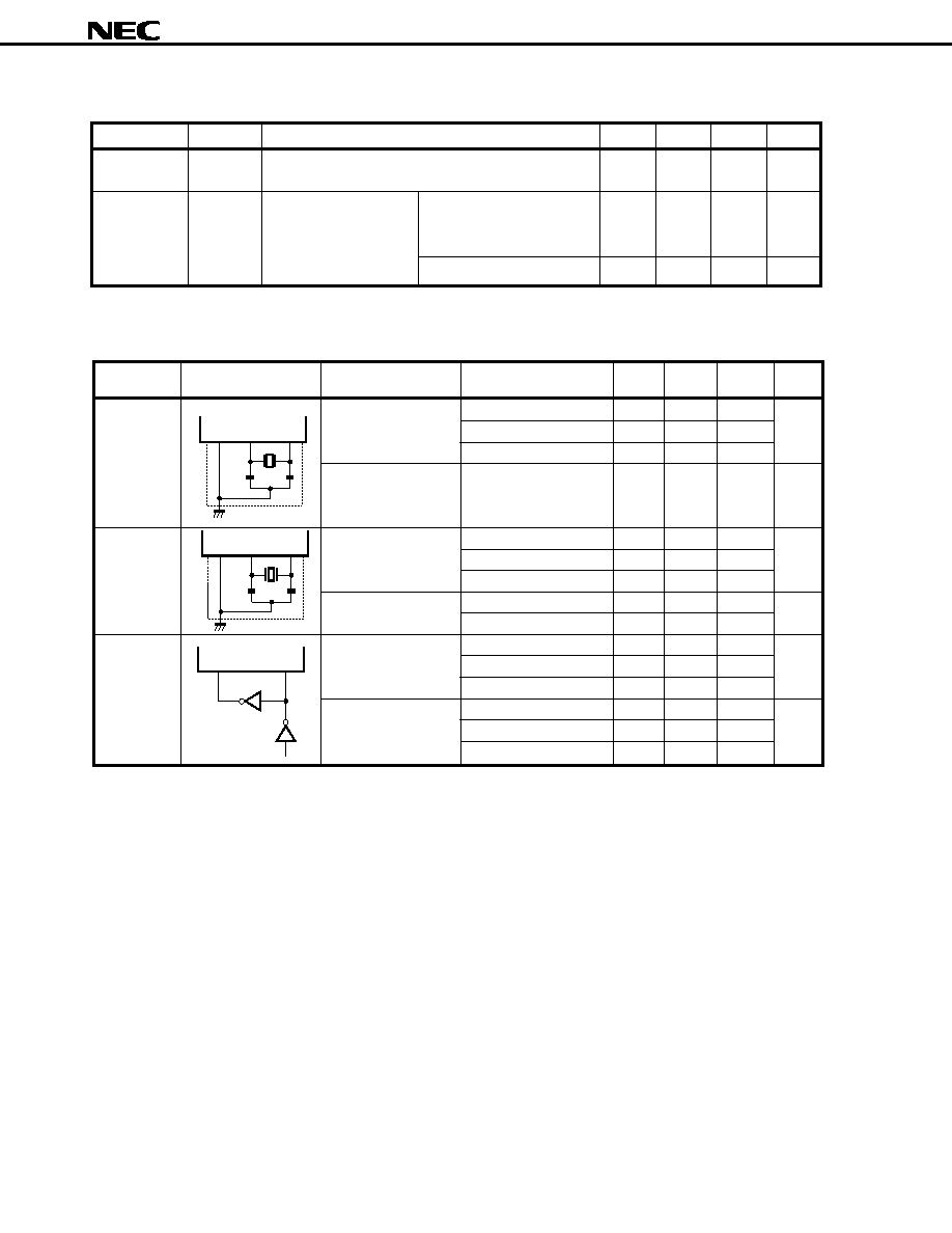
Main System Clock Oscillator Characteristics (TA = –40 to +85
°C, VDD = 1.8 to 5.5 V)
Resonator
Recommended
Parameter
Conditions
MIN.
TYP.
MAX.
Unit
Circuit
Ceramic
Oscillation
4.5 V
≤ VDD ≤ 5.5 V
1.0
12.0
MHz
resonator
frequency (fX)Note 1
3.0 V
≤ VDD < 4.5 V
1.0
8.38
1.8 V
≤ VDD < 3.0 V
1.0
5.0
Oscillation
After VDD reaches
4
ms
stabilization timeNote 2
oscillation voltage range
MIN.
Crystal
Oscillation
4.5 V
≤ VDD ≤ 5.5 V
1.0
12.0
MHz
resonator
frequency (fX)Note 1
3.0 V
≤ VDD < 4.5 V
1.0
8.38
1.8 V
≤ VDD < 3.0 V
1.0
5.0
Oscillation
4.0 V
≤ VDD ≤ 5.5 V
10
ms
stabilization timeNote 2
1.8 V
≤ VDD < 4.0 V
30
External
X1 input
4.5 V
≤ VDD ≤ 5.5 V
1.0
12.0
MHz
clock
frequency (fX)Note 1
3.0 V
≤ VDD < 4.5 V
1.0
8.38
1.8 V
≤ VDD < 3.0 V
1.0
5.0
X1 input
4.5 V
≤ VDD ≤ 5.5 V
38
500
ns
high-/low-level width
3.0 V
≤ VDD < 4.5 V
50
500
(tXH, tXL)
1.8 V
≤ VDD < 3.0 V
85
500
Notes 1. Indicates only oscillator characteristics. Refer to AC Characteristics for instruction execution time.
2. Time required to stabilize oscillation after reset or STOP mode release.
Cautions
1. When using the main system clock oscillator, wire as follows in the area enclosed by the broken
lines in the above figures to avoid an adverse effect from wiring capacitance.
Keep the wiring length as short as possible.
Do not cross the wiring with the other signal lines.
Do not route the wiring near a signal line through which a high fluctuating current flows.
Always make the ground point of the oscillator capacitor the same potential as VSS1.
Do not ground the capacitor to a ground pattern through which a high current flows.
Do not fetch signals from the oscillator.
2. When the main system clock is stopped and the system is operating on the subsystem clock,
wait until the oscillation stabilization time has been secured by the program before switching
back to the main system clock.
Capacitance (TA = 25
°C, VDD = VSS = 0 V)
Parameter
Symbol
Conditions
MIN.
TYP.
MAX.
Unit
Input
CIN
f = 1 MHz
15
pF
capacitance
Unmeasured pins returned to 0 V.
I/O
CIO
f = 1 MHz
P00 to P03, P20 to P25,
15
pF
capacitance
Unmeasured pins
P34 to P36, P40 to P47,
returned to 0 V.
P50 to P57, P64 to P67,
P70 to P75
P30 to P33
20
pF
Remark
Unless otherwise specified, the characteristic of alternate-function pins are the same as those of port pins.
C2
C1
X1
X2
IC
C2
C1
X1
X2
IC
X2
X1
相關(guān)PDF資料 |
PDF描述 |
|---|---|
| UPD78011HGK-XXX-8A8 | 8-BIT, MROM, 10 MHz, MICROCONTROLLER, PQFP64 |
| UPD78053GC-XXX-8BT | 8-BIT, MROM, 5 MHz, MICROCONTROLLER, PQFP80 |
| UPD78322GJ-XXX-5BJ | 16-BIT, MROM, 16 MHz, MICROCONTROLLER, PQFP74 |
| UPD789132GS-XXX | 8-BIT, MROM, MICROCONTROLLER, PDSO30 |
| UPD789122UC-XXX-5A4 | 8-BIT, MROM, MICROCONTROLLER, PDSO30 |
相關(guān)代理商/技術(shù)參數(shù) |
參數(shù)描述 |
|---|---|
| UPD780024AGK-C42-9ET | 制造商:Renesas Electronics Corporation 功能描述: |
| UPD780024AGK-C93-9ET | 制造商:Renesas Electronics Corporation 功能描述: |
| UPD780033AGK-B03-9ET | 制造商:Renesas Electronics Corporation 功能描述: |
| UPD780033AGK-B03-9ET-A | 制造商:Renesas Electronics Corporation 功能描述: |
| UPD780034AGC-119-8BS-A | 制造商:Renesas Electronics Corporation 功能描述:NECUPD780034AGC-119-8BS-A MCU |
發(fā)布緊急采購(gòu),3分鐘左右您將得到回復(fù)。