- 您現(xiàn)在的位置:買賣IC網(wǎng) > PDF目錄379501 > UPD750006A (NEC Corp.) 4 BIT SINGLE-CHIP MICROCONTROLLER PDF資料下載
參數(shù)資料
| 型號: | UPD750006A |
| 廠商: | NEC Corp. |
| 英文描述: | 4 BIT SINGLE-CHIP MICROCONTROLLER |
| 中文描述: | 4位單片機 |
| 文件頁數(shù): | 59/84頁 |
| 文件大小: | 719K |
| 代理商: | UPD750006A |
第1頁第2頁第3頁第4頁第5頁第6頁第7頁第8頁第9頁第10頁第11頁第12頁第13頁第14頁第15頁第16頁第17頁第18頁第19頁第20頁第21頁第22頁第23頁第24頁第25頁第26頁第27頁第28頁第29頁第30頁第31頁第32頁第33頁第34頁第35頁第36頁第37頁第38頁第39頁第40頁第41頁第42頁第43頁第44頁第45頁第46頁第47頁第48頁第49頁第50頁第51頁第52頁第53頁第54頁第55頁第56頁第57頁第58頁當前第59頁第60頁第61頁第62頁第63頁第64頁第65頁第66頁第67頁第68頁第69頁第70頁第71頁第72頁第73頁第74頁第75頁第76頁第77頁第78頁第79頁第80頁第81頁第82頁第83頁第84頁
59
μ
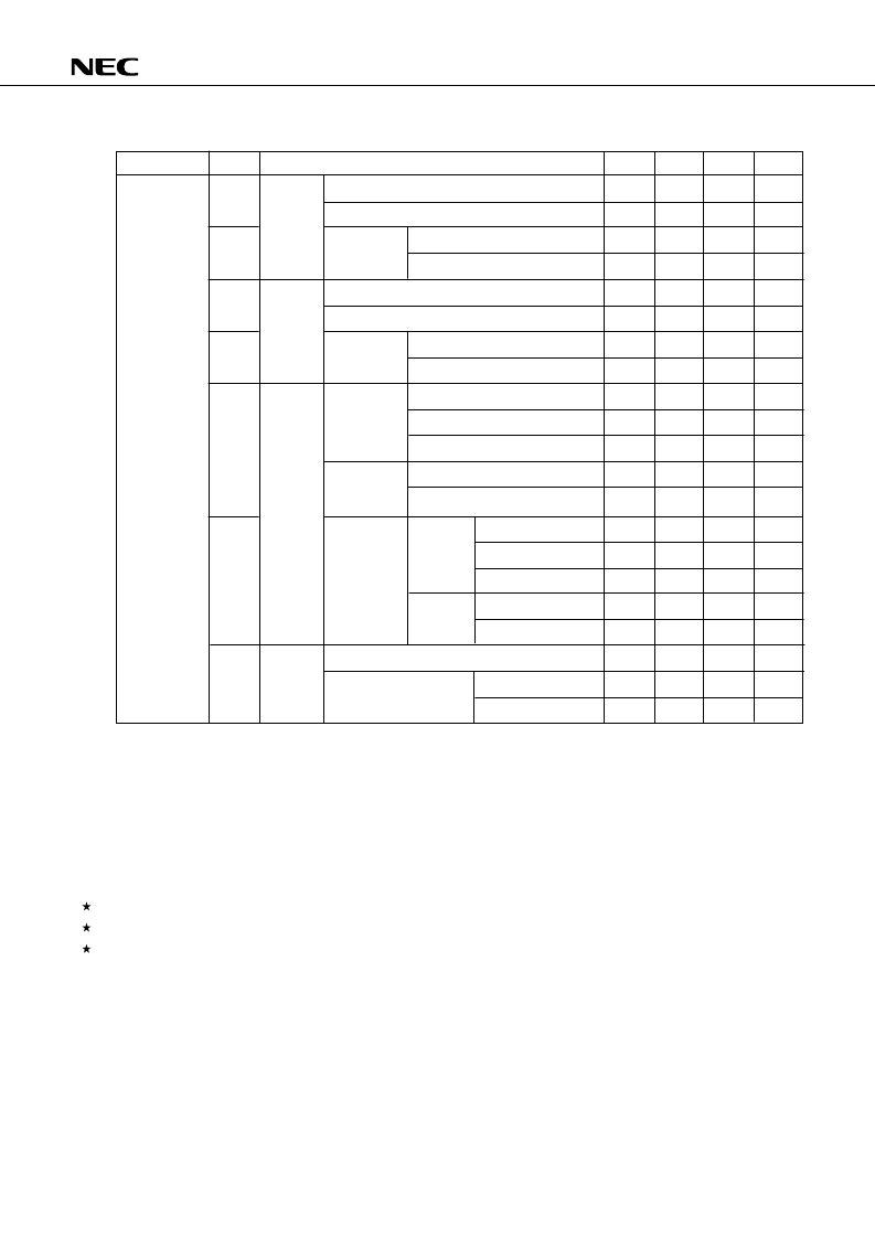
PD750004, 750006, 750008, 750004(A), 750006(A), 750008(A)
Parameter
Power supply
current
Note 1
Min.
Conditions
6.0
MHz
Note 2
crystal
C1 = C2 =
22 pF
4.19
MHz
Note 2
crystal
C1 = C2 =
22 pF
32.768
kHz
Note 5
crystal
V
DD
= 5.0 V
±
10%
V
DD
= 3.0 V
±
10 %
V
DD
= 5.0 V
±
10%
V
DD
= 3.0 V
±
10%
V
DD
= 3.0 V
±
10%
V
DD
= 2.5 V
±
10%
V
DD
= 3.0 V, T
A
= 25
°
C
V
DD
= 3.0 V
±
10%
V
DD
= 3.0 V, T
A
= 25
°
C
Low-current-
drain
mode
Note 7
DC CHARACTERISTICS
(T
A
= -40 to +85
°
C, V
DD
= 2.2 to 5.5 V)
Notes 1.
This current excludes the current which flows through the built-in pull-up resistors.
2.
This value applies also when the subsystem clock oscillates.
3.
Value when the processor clock control register (PCC) is set to 0011 and the
μ
PD750008 is operated in
the high-speed mode.
4.
Value when the PCC is set to 0000 and the
μ
PD750008 is operated in the low-speed mode.
5.
This value applies when the system clock control register (SCC) is set to 1001 to stop the main system
clock pulse and to start the subsystem clock pulse.
6.
Mode when the sub-oscillator control register (SOS) is set to 0000.
7.
Mode when the SOS is set to 0010.
8.
This value applies when the SOS is set to 00
×
1 and the sub-oscillator feedback resistor is not used (
×
=
don’t care).
Symbol
I
DD1
I
DD2
I
DD1
I
DD2
I
DD3
I
DD4
I
DD5
Typ.
1.9
0.4
0.72
0.27
1.5
0.25
0.7
0.23
12
7
12
6
6
8.5
5
8.5
3.5
3.5
0.05
0.02
0.02
Max.
6.0
1.3
2.1
0.8
4.0
0.75
2.0
0.7
35
21
24
18
12
25
15
17
12
7
10
5
3
Unit
mA
mA
mA
mA
mA
mA
mA
mA
μ
A
μ
A
μ
A
μ
A
μ
A
μ
A
μ
A
μ
A
μ
A
μ
A
μ
A
μ
A
μ
A
V
DD
= 5.0 V
±
10%
Note 3
V
DD
= 3.0 V
±
10%
Note 4
HALT mode
V
DD
= 5.0 V
±
10%
Note 3
V
DD
= 3.0 V
±
10%
Note 4
HALT mode
Low-voltage
mode
Note 6
HALT mode
Low-volt-
age
mode
Note 6
V
DD
= 5.0 V
±
10%
V
DD
= 3.0 V
±
10%
Low-cur-
rent-drain
mode
Note 7
XT1 =
0 V
Note 8
STOP
mode
V
DD
= 3.0 V
±
10%
V
DD
= 2.5 V
±
10%
V
DD
= 3.0 V, T
A
= 25
°
C
V
DD
= 3.0 V
±
10%
V
DD
= 3.0 V, T
A
= 25
°
C
T
A
= 25
°
C
相關(guān)PDF資料 |
PDF描述 |
|---|---|
| UPD750006CU | 4 BIT SINGLE-CHIP MICROCONTROLLER |
| UPD750006CUA | 4 BIT SINGLE-CHIP MICROCONTROLLER |
| UPD750006GB | 4 BIT SINGLE-CHIP MICROCONTROLLER |
| UPD75104A | 4-BIT SINGLE-CHIP MICROCOMPUTER |
| UPD75104AGC | 4-BIT SINGLE-CHIP MICROCOMPUTER |
相關(guān)代理商/技術(shù)參數(shù) |
參數(shù)描述 |
|---|---|
| UPD750068GT-396 | 制造商:Renesas Electronics Corporation 功能描述: |
| UPD7507C189 | 制造商:Panasonic Industrial Company 功能描述:IC |
| UPD7508CU265 | 制造商:Panasonic Industrial Company 功能描述:IC |
| UPD75208 | 制造商:Panasonic Industrial Company 功能描述:IC |
| UPD753012AGC-P33-8BT-A | 制造商:Renesas Electronics Corporation 功能描述: |
發(fā)布緊急采購,3分鐘左右您將得到回復。