- 您現(xiàn)在的位置:買賣IC網(wǎng) > PDF目錄361546 > UF640-TF3-T (UNISONIC TECHNOLOGIES CO LTD) 18 A, 200 V, 0.18 OHM, N-CHANNEL POWER MOSFET PDF資料下載
參數(shù)資料
| 型號(hào): | UF640-TF3-T |
| 廠商: | UNISONIC TECHNOLOGIES CO LTD |
| 元件分類: | JFETs |
| 英文描述: | 18 A, 200 V, 0.18 OHM, N-CHANNEL POWER MOSFET |
| 中文描述: | 18 A, 200 V, 0.18 ohm, N-CHANNEL, Si, POWER, MOSFET, TO-220AB |
| 封裝: | TO-220F, 3 PIN |
| 文件頁(yè)數(shù): | 2/5頁(yè) |
| 文件大?。?/td> | 149K |
| 代理商: | UF640-TF3-T |
UF640
MOSFET
UNISONIC TECHNOLOGIES CO., LTD
www.unisonic.com.tw
2 of 5
Ver.A
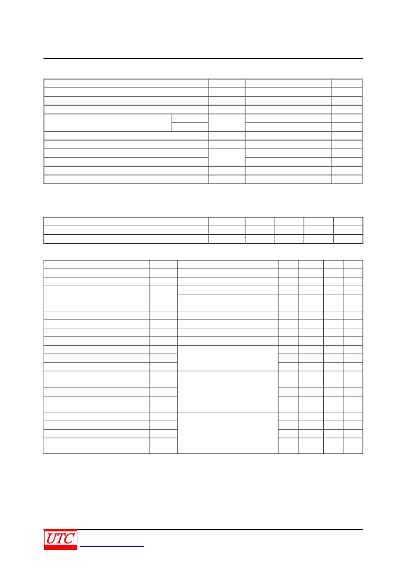
ABS OLUT E MAX IMUM RAT ING
(T
C
= 25
, unless otherwise specified)
PARAMETER
SYMBOL
V
DSS
V
DGR
V
GSS
RATINGS
200
200
±20
18
11
72
580
125
1.0
+150
-55 ~ +150
UNIT
V
V
V
A
A
A
mJ
W
W/
Drain Source Voltage
Drain Gate Voltage (R
GS
= 20k
)
Gate Source Voltage
T
C
= 25
T
C
= 100
Continuous Drain Current
I
D
Pulsed Drain Current (Note )
Single Pulse Avalanche Energy Rating (Note )
Maximum Power Dissipation
Dissipation Derating Factor
Junction Temperature
Storage Temperature
Note Absolute maximum ratings are those values beyond which the device could be permanently damaged.
Absolute maximum ratings are stress ratings only and functional device operation is not implied.
I
DM
E
AS
P
D
T
J
T
STG
T HERMAL DAT A
PARAMETER
SYMBOL
θ
JA
θ
JC
MIN
TYP
MAX
62
1
UNIT
°C/W
°C/W
Thermal Resistance, Channel to Ambient
Thermal Resistance, Channel to Case
ELECT RICAL CHARACT ERIS T ICS
(T
C
= 25
, unless otherwise specified)
PARAMETER
SYMBOL
BV
DSS
V
GS(THR)
V
GS
= V
DS
, I
D
= 250μA
V
DS
= Rated BV
DSS
, V
GS
= 0V
I
DSS
V
DS
= 0.8 x Rated BV
DSS
, V
GS
= 0V,
T
J
= 125
I
D(ON)
V
DS
>I
D(ON)
x R
DS(ON)
MAX, V
GS
= 10V
I
GSS
V
GS
= ±20V
R
DS(ON)
I
D
= 10A, V
GS
= 10V
g
FS
V
DS
≥
10V, I
D
= 11A
C
ISS
C
OSS
C
RSS
V
GS
= 10V, I
D
≈
18A, V
DS
= 0.8 x
Rated BV
DSS
Gate Charge is
Essentially Independent of
Operating Temperature I
G(REF)
=
1.5mA
t
D(ON)
t
R
t
D(OFF)
MOSFET Switching Times are
Essentially Independent of
Operating Temperature
TEST CONDITIONS
I
D
= 250μA, V
GS
= 0V
MIN
200
2
TYP
MAX
UNIT
V
V
μA
Drain Source Breakdown Voltage
Gate Threshold Voltage
4
25
Drain-Source Leakage Current
250
μA
On-State Drain Current
Gate-Source Leakage Current
Drain-Source On Resistance
Forward Transconductance
Input Capacitance
Output Capacitance
Reverse Transfer Capacitance
Total Gate Charge
(Gate to Source + Gate to Drain)
Gate-Source Charge
18
6.7
A
nA
S
pF
pF
pF
±100
0.18
0.14
10
1275
400
100
V
DS
= 25V, V
GS
= 0V, f = 1MHz
Q
G(TOT)
43
64
nC
Q
GS
8
nC
Gate-Drain “Miller” Charge
Q
GD
22
nC
Turn-On Delay Time
Rise Time
Turn-Off Delay Time
13
50
46
21
77
68
ns
ns
ns
Fall Time
t
F
V
DD
= 100V, I
D
≈
18A, R
GS
= 9.1
,
R
L
= 5.4
,
35
54
ns
相關(guān)PDF資料 |
PDF描述 |
|---|---|
| UF730 | 5.5A, 400V, 1.0 OHM, N-CHANNEL POWER MOSFET |
| UF730L-TA3-T | 5.5A, 400V, 1.0 OHM, N-CHANNEL POWER MOSFET |
| UF730L-TF3-T | 5.5A, 400V, 1.0 OHM, N-CHANNEL POWER MOSFET |
| UF730-TA3-T | 5.5A, 400V, 1.0 OHM, N-CHANNEL POWER MOSFET |
| UF730-TF3-T | 5.5A, 400V, 1.0 OHM, N-CHANNEL POWER MOSFET |
相關(guān)代理商/技術(shù)參數(shù) |
參數(shù)描述 |
|---|---|
| UF64RED | 制造商:Siemens 功能描述:End feed red |
| UF69-30A | 制造商:The Cherry Corporation 功能描述:SWITCH SPDT SNAP-IN |
| UF730 | 制造商:UTC-IC 制造商全稱:UTC-IC 功能描述:5.5 Amps, 400 Volts N-CHANNEL POWER MOSFET |
| UF730_10 | 制造商:UTC-IC 制造商全稱:UTC-IC 功能描述:5.5 Amps, 400 Volts N-CHANNEL POWER MOSFET |
| UF730G-TA3-T | 制造商:UTC-IC 制造商全稱:UTC-IC 功能描述:5.5 Amps, 400 Volts N-CHANNEL POWER MOSFET |
發(fā)布緊急采購(gòu),3分鐘左右您將得到回復(fù)。