- 您現(xiàn)在的位置:買賣IC網(wǎng) > PDF目錄378722 > UCC1858 (Texas Instruments, Inc.) High Efficiency, High Power Factor Preregulator PDF資料下載
參數(shù)資料
| 型號: | UCC1858 |
| 廠商: | Texas Instruments, Inc. |
| 元件分類: | 基準電壓源/電流源 |
| 英文描述: | High Efficiency, High Power Factor Preregulator |
| 中文描述: | 高效率,高功率因數(shù)前置穩(wěn)壓器 |
| 文件頁數(shù): | 4/12頁 |
| 文件大小: | 343K |
| 代理商: | UCC1858 |
4
UCC1858
UCC2858
UCC3858
PIN DESCRIPTIONS
CA–:
(Current Amplifier Inverting Input) This input and
the non-inverting input MOUT remain functional down to
GND.
CAO:
(Current Amplifier Ouput) Output of a wide band-
width amplifier that senses line current and commands
the pulse width modulator (PWM) to force the correct cur-
rent. This output can swing close to GND, allowing the
PWM to force zero duty cycle when necessary.
CRMS:
(RMS Measurement Capacitor) A capacitor con-
nected between CRMS and GND enables averaging of
the AC line voltage over a half cycle. IAC current is inter-
nally mirrored to provide charging current for CRMS.
CT:
(Oscillator Timing Capacitor) A capacitor from CT to
GND will set the free-running PWM oscillator frequency
according to:
0814
.
f
R
C
T
T
=
FBL:
(Frequency Foldback Level Select) Selects the level
of the voltage error amplifier output at which frequency
foldback begins. A chip shutdown can be attained by
bringing the foldback level pin to below 0.5V.
FBM:
(Minimum Frequency Reference) A resistor be-
tween this pin and VREF is used to set the minimum fre-
quency during foldback mode. Once the value of R
T
and
C
T
are determined, use
0857
.
R
C
f
R
FBM
T
MIN
T
=
to find the value of R
FBM
which will set the minimum
foldback frequency to f
MIN.
This pin also incorporates a
foldback override which enables the part to return quickly
to normal operating mode when the load comes back up.
To override foldback mode, force this pin below 1.5V with
an open collector.
GND:
(Ground) All voltages measured with respect to
ground. VDD and VREF should be bypassed directly to
GND with a 0.1
μ
F or larger ceramic capacitor. The timing
capacitor discharge current also returns to this pin, so
the lead from CT to GND should be as short and direct
as possible.
IAC:
(Input AC Current) This input to the analog multiplier
is a current. The multiplier is tailored for very low distor-
tion from this current input (I
IAC
) to MOUT. Requires
some bypassing to GND for noise filtering (<470pF).
MOUT:
(Multiplier Output) The output of the analog multi-
plier and the non-inverting input of the current amplifier
are connected together at MOUT. As the multiplier output
is a current, this is a high impedance input so the ampli-
fier can be configured as a differential amplifier to reject
ground noise. The voltage at this pin is also used to im-
plement peak current limiting.
OUT:
(Gate Drive Output) The output of the PWM is a to-
tem pole MOSFET gate driver. A series gate resistor of
at least 5
is recommended to prevent interaction be-
tween the gate impedance and the output driver that
might cause the gate drive to overshoot excessively.
RT:
(Oscillator Timing Resistor) A resistor from RT to
GND is used to program oscillator discharge current.
SYNC:
(Oscillator Synchronization Input) Allows the PFC
to be synchronized to a trailing edge modulator in the
DC-DC stage. A synchronization pulse can be generated
from the positive output edge of the downstream regula-
tor and applied to this pin. The internal clock is reset
(charged up) on the rising edge of the SYNC input.
VA–:
(Voltage Amplifier Inverting Input) This pin is nor-
mally connected to the boost converter output through a
divider network. It also is an input to the overvoltage
comparator where by the output is terminated if this pin’s
voltage exceeds 3.15V.
VAO:
transconductance amplifier that regulates output voltage.
The voltage amplifier output is internally limited to ap-
proximately 6V for power limiting. It is also used to deter-
mine
the
frequency
foldback
network is connected from this pin to GND.
(Voltage
Amplifier
Output)
Output
of
the
mode. Compensation
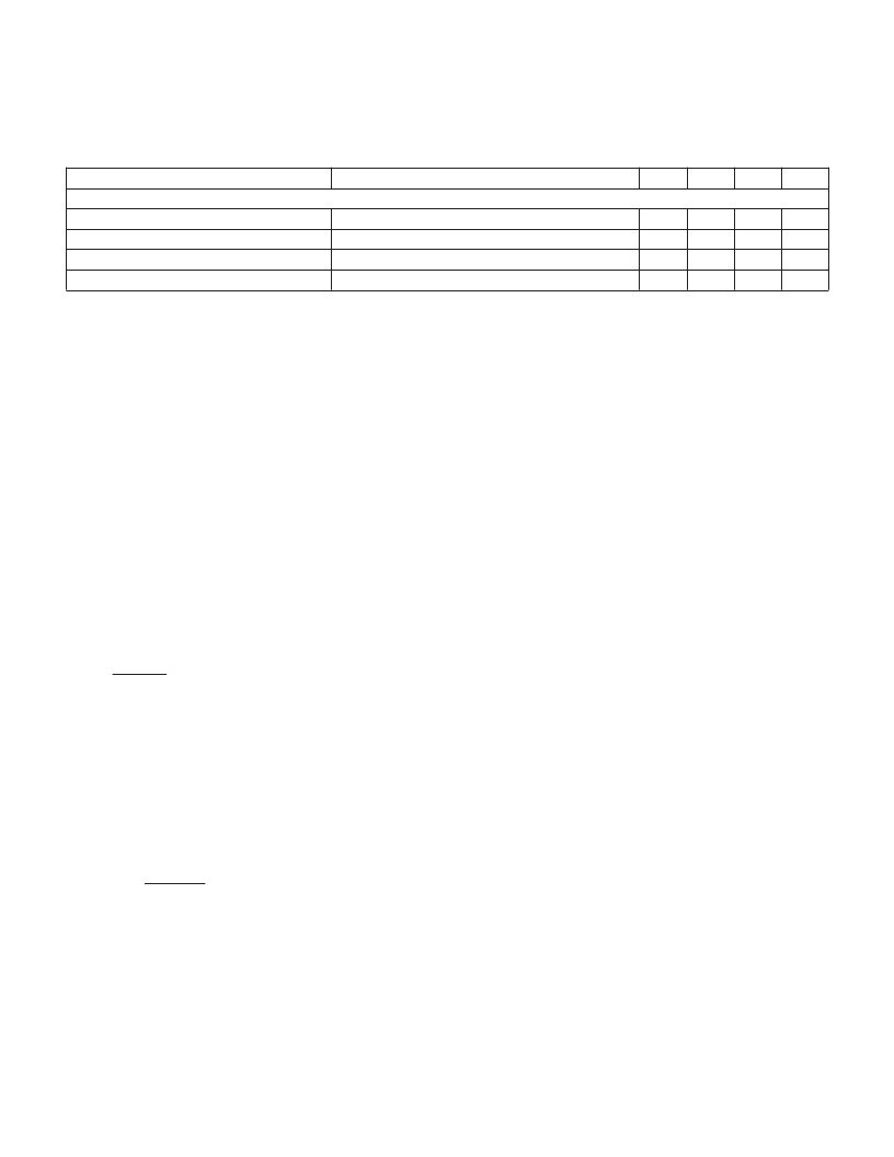
ELECTRICAL CHARACTERISTICS:
Unless otherwise stated, these specifications apply for T
A
= 0°C to 70°C for the
UCC3858, –40°C to +85°C for the UCC2858, and –55°C to +150°C for the UCC1858, V
VDD
= 12V, R
T
= 24k, C
T
= 330pF, R
FBM
=
96k, I
IAC
= 100
μ
A, T
A
= T
J
.
PARAMETER
TEST CONDITIONS
Gate Driver
Pull Up Resistance
I
OUT
= 100mA
Pull Down Resistance
I
OUT
= –100mA
Output Rise Time
C
LOAD
= 1nF, R
S
= 10
Output Fall Time
C
LOAD
= 1nF, R
S
= 10
MIN
TYP
MAX
UNITS
7
ns
ns
3.5
25
20
Note1: M
OUT
current with contributions form CA+ and peak limit level shift subtracted out.
相關(guān)PDF資料 |
PDF描述 |
|---|---|
| UCC1884 | Frequency Foldback Current Mode PWM Controller |
| UCC2884 | Frequency Foldback Current Mode PWM Controller |
| UCC1888 | Off-line Power Supply Controller |
| UCC2888 | Off-line Power Supply Controller |
| UCC1926 | 【 20A Integrated Current Sensor |
相關(guān)代理商/技術(shù)參數(shù) |
參數(shù)描述 |
|---|---|
| UCC1858DW | 制造商:未知廠家 制造商全稱:未知廠家 功能描述:Power Factor Controller |
| UCC1858DWTR | 制造商:未知廠家 制造商全稱:未知廠家 功能描述:Power Factor Controller |
| UCC1858J | 制造商:未知廠家 制造商全稱:未知廠家 功能描述:Power Factor Controller |
| UCC1858N | 制造商:未知廠家 制造商全稱:未知廠家 功能描述:Analog IC |
| UCC1883J | 制造商:未知廠家 制造商全稱:未知廠家 功能描述:Current-Mode SMPS Controller |
發(fā)布緊急采購,3分鐘左右您將得到回復(fù)。