- 您現(xiàn)在的位置:買賣IC網 > PDF目錄382720 > UCB1300 (NXP Semiconductors N.V.) Advanced modem/audio analog front-end PDF資料下載
參數資料
| 型號: | UCB1300 |
| 廠商: | NXP Semiconductors N.V. |
| 英文描述: | Advanced modem/audio analog front-end |
| 中文描述: | 先進的調制解調器/音頻模擬前端 |
| 文件頁數: | 20/56頁 |
| 文件大小: | 1022K |
| 代理商: | UCB1300 |
第1頁第2頁第3頁第4頁第5頁第6頁第7頁第8頁第9頁第10頁第11頁第12頁第13頁第14頁第15頁第16頁第17頁第18頁第19頁當前第20頁第21頁第22頁第23頁第24頁第25頁第26頁第27頁第28頁第29頁第30頁第31頁第32頁第33頁第34頁第35頁第36頁第37頁第38頁第39頁第40頁第41頁第42頁第43頁第44頁第45頁第46頁第47頁第48頁第49頁第50頁第51頁第52頁第53頁第54頁第55頁第56頁

1999 Jul 20
20
Philips Semiconductors
Preliminary specification
Advanced modem/audio analog front-end
UCB1300
10 BIT ADC
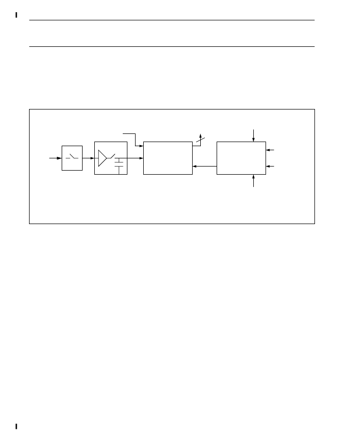
The UCB1300 includes a 10 bit successive approximation analog to digital converter (ADC) with built-in track and hold
circuit and an analog multiplexer to select one of the 4 analog inputs (AD0 - AD3), the 4 touch screen inputs (TSPX,
TSMX, TSPY, TSMY) or the pressure output of the touch screen bias circuit. The ADC is used to read-out the touch
screen inputs and it measures the voltage on the four analog high voltage inputs AD0 - AD3. The analog multiplexer
contains 4 resistive dividers to attenuate the high voltage on the AD0 - AD3 inputs to the ADC input range.
The ADC is controlled completely through the SIB interface, but the UCB1300 contains internal logic to ease the control
of the ADC and to minimize the number of SIB frame read/write actions.
A complete ADC control sequence analog to digital conversion consists of several phases. Firstly the ADC has to be
enabled, secondly the input selector must be set to the proper input, thirdly the ADC conversion has to be started and
finally the ADC result has to be read from register 11.
The ADC is activated by setting ADC_ENA in register 10. The ADC circuit, including the track and hold circuit does not
consume any power as long as this bit is reset. The analog input multiplexer is controlled by ADC_INPUT[n] and the ADC
is actually started with the ADC_START bit. When TSPXand TSMX are in the interrupt mode, the ADC cannot be started,
even to measure AD0-3.
The UCB1300 has two different modes to start the ADC conversion, which are selected by the ADC_SYNC_ENA bit.
The default mode is the non-synchronization mode, in which the conversion is started directly with a 0->1 transition of
ADC_START. Secondly the ADC is started at a rising edge of the signal applied to the ADCSYNC pin if
ADC_SYNC_ENA is set. Activating the ADC while keeping the start logic in the started state (ADC_START = 1) will lead
to unpredictible behavior and the value of the ADC data register will not be meaningfull. Always activate a start sequence
for each aquisition (0 to 1 transition on the internal ADC_START signal).
The internal track and hold circuit requires a certain settling time to track the input signal correctly. This can be ensured
from the software by writing first a SIB frame with the ADC multiplexer setting before the SIB frame with the ADC_START
command is transferred. The UCB1300 ADC start/stop logic will detect whether the ADC input multiplexer is changed in
the same SIB frame as the ADC start command is given. In that case it will delay the actual start of the ADC circuit to
ensure that the track and hold settling time requirements are met. This leads to the following two timing diagrams:
Fig.13 Block diagram of the 10-bit ADC circuit.
internal reference
mux
9 to 1
track&hold
10 bit ADC
to control reg 11
10
ADC start
adcsync
stop logic
adc start
sync
enable
adc_sync_ena
相關PDF資料 |
PDF描述 |
|---|---|
| UCB1300BE | Advanced modem/audio analog front-end |
| UCB1400BE | Audio codec with touch screen controller and power management monitor |
| UCB1400 | Audio codec with touch screen controller and power management monitor |
| UCB1500 | PCI to AC97 bridge/host controller |
| UCC1913D | Very low drop voltage regulators with inhibit |
相關代理商/技術參數 |
參數描述 |
|---|---|
| UCB1300BE | 制造商:PHILIPS 制造商全稱:NXP Semiconductors 功能描述:Advanced modem/audio analog front-end |
| UCB1400 | 制造商:PHILIPS 制造商全稱:NXP Semiconductors 功能描述:Audio codec with touch screen controller and power management monitor |
| UCB1400BE | 制造商:PHILIPS 制造商全稱:NXP Semiconductors 功能描述:Audio codec with touch screen controller and power management monitor |
| UCB1400BE,128 | 功能描述:接口—CODEC AUDIO CODEC WITH TOUCHSCREEN RoHS:否 制造商:Texas Instruments 類型: 分辨率: 轉換速率:48 kSPs 接口類型:I2C ADC 數量:2 DAC 數量:4 工作電源電壓:1.8 V, 2.1 V, 2.3 V to 5.5 V 最大工作溫度:+ 85 C 安裝風格:SMD/SMT 封裝 / 箱體:DSBGA-81 封裝:Reel |
| UCB1400BE,151 | 功能描述:接口—CODEC AUDIO CODEC RoHS:否 制造商:Texas Instruments 類型: 分辨率: 轉換速率:48 kSPs 接口類型:I2C ADC 數量:2 DAC 數量:4 工作電源電壓:1.8 V, 2.1 V, 2.3 V to 5.5 V 最大工作溫度:+ 85 C 安裝風格:SMD/SMT 封裝 / 箱體:DSBGA-81 封裝:Reel |
發(fā)布緊急采購,3分鐘左右您將得到回復。